BF52x学习
来源:互联网 发布:美国网络小说 知乎 编辑:程序博客网 时间:2024/04/19 11:22
BF527:
处理器主频最高600MHz,外设频率最高133MHz,RISC处理器,
片上内存132K byte,支持SDRAM和异步8 或16 bit控制器,
启动选择灵活,可从外部FLASH,SPI,TWI 或者主机设备的SPI,TWI,UART.
使用一次性可编程内存保护代码安全,
内存管理单元提供内存保护功能,
支持USB2.0并集成802.3标准以太网控制器。
并行外设接口PPI,支持ITU-R 656 视频数据格式
2个双通道全双工SPORTS接口,支持立体声I2S通道
一个主机DMA接口,12外设DMA通道,包含2个以太网DMA通道,2个内存到内存DMA通道,
1个SPI接口,2个UART接口支持IRDA,一个2线接口(TWI)控制器
8个32位定时器/计数器支持PWM;48个GPIO,一个NFC NAND FLASH 控制器接口,jtag
片上PLL
关于GPIO
共48个GPIO,但大部分有复用功能,默认情况下,PF,PG,PH,处于GPIO模式,PJ不提供GPIO功能,在GPIO模式中,该引脚可配置为数据输入,数据输出和中断输入,复用功能必须先设置PORTF_FER, PORTG_FER, PORTH_FER寄存器。然后设置复用控制寄存器PORTF_MUX, PORTG_MUX, PORTH_MUX。
PF结构
PORT F复用功能如下图所示,PF功能受PORTF_FER,PORTF_MUX寄存器控制。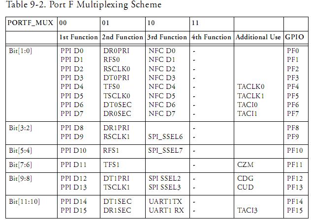
PORTF_MUX 寄存器的Bit 12 位是Port J 的 PPICLK/TMRCLK 引脚的输入使能控制位,置1 使能,置0 禁止, PORTF_MUX 寄存器的Bit 13-15 位保留。
PORT G结构
PORT G复用功能如下图所示,PG功能受PORTG_FER,PORTG_MUX寄存器控制。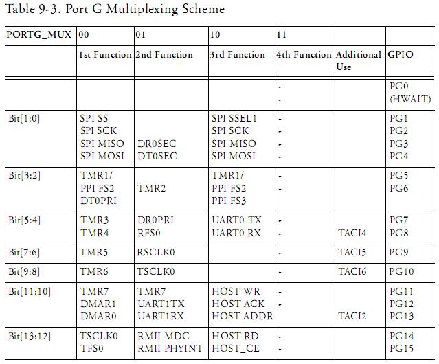
When TMR6 is an output, SPORT0 ignores the external TSCLK0 signal on PG14.Special attention is required for the use of the timers with PPI enabled.Timer 0 and Timer 1 are typically used for PPI frame sync generation.
Any GPIO can be enabled individually and overrides the peripheral function if the respective bit in the PORTG_FER is cleared.
Bits 14-15 in the PORTG_MUX register are reserved.
PH结构
PORT H复用功能如下图所示,PH功能受PORTH_FER,PORTH_MUX寄存器控制。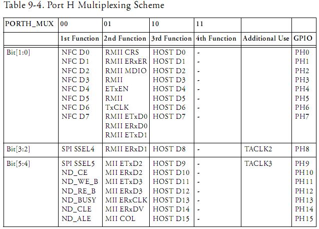
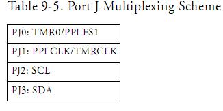
PORT J结构
PJ不提供GPIO功能,但提供对TWI信号的支持,
The PPICLK/TMRCLK pin is enabled by setting bit 12 in the PORTF_MUX register.
Input Tap Considerations
When input taps (as well as GPIO based taps) are used with other functionality enabled on the GPIO pins, the signals seen by the input tap modules might be different from what is seen on the pins. This is because different pin functions have different signal requirements with respect to when the signal is latched, if at all. Because of this, input taps multiplexed on certain pins may behave differently than those on other pins, depending on which pin function is selected. The input taps will see different signals than at the pins in the following cases:
* All GPIO inputs except PG0, PG1, PG2, PG9, PG10, PG11, PG12, PG13, PG14, PH3, PH4, PH5, PH7, PH9, PH11, PH13, PH15 when GPIO is tapped with PORTx_FER set to 1.
*TACLK0 if PORTF_FER[4] = 1 and PORTF_MUX[1:0] = b#00 or b#01
*TACLK1 if PORTF_FER[5] = 1 and PORTF_MUX[1:0] = b#00
*TACI0 if PORTF_FER[6] = 1 and PORTF_MUX[1:0] = b#00 or b#01
*TACI1 if PORTF_FER[7] = 1 and PORTF_MUX[1:0] = b#00 or b#01
* CZM if PORTF_FER[11] = 1 and PORTF_MUX[7:6] = b#00 or b#01
* CDG if PORTF_FER[12]= 1 and PORTF_MUX[9:8] = b#00 or b#01
*CUD if PORTF_FER[13] = 1 and PORTF_MUX[9:8] = b#00
*TACI3 if PORTF_FER[15] = 1 and PORTF_MUX[11:10] = b#00 or b#01
* TACI4 if PORTG_FER[8] = 1 and PORTG_MUX[5:4] = b#01
*TACLK2 if PORTH_FER[8] = 1 and PORTH_MUX[3:2] = b#01
PF,PG,PH,PJ使用系统时钟工作,当配置这48个GPIO为输出时,传输数据时钟应该是系统时钟的分频,
当配置为输入的时候,设计系统应考虑核心时钟与系统时钟之间潜在的等待时间,改变port 引脚状态时,处理器核心在3个
系统时钟周期后 才能觉察到。当配置为中断输入时(通过电平的高低进行判断中断的存在)When configured for level-sensitive interrupt generation, there is a minimum latency of 4 SCLK cycles between the time the signal is asserted on the pin and the time that program flow is interrupted. When configured for edge-sensitive interrupt generation, an additional SCLK cycle of latency is introduced, giving a total latency of 5 SCLK cycles between the time the edge is asserted and the time that the core program flow is interrupted.
通过设置外设使能寄存器PORTx_PER控制GPIO的功能,当控制位清除时,处于GPIO模式,若设置GPIO的输出模式,需设置相应的方向位(在PORTxIO_DIR寄存器中),配置引脚处于数据输入或中断输入时,需使能相应的PORTxIO_INEN寄存器位。
默认情况下,复位后所有的外设引脚被配置为输入,PF、PG、PH的引脚处于GPIO模式,但GPIO模式的输入功能被禁止,需要上拉电阻。
当在寄存器PORTx_PER中的控制位被置位,该引脚处于外设功能模式,不在受GPIO模式的控制,但GPIO模块仍然可以察觉引脚状态的变化,当使用特定外设接口时,有关该外设使用的引脚必须全部使能,保证清除不必要的控制位。
GPIO模式
在共48个GPIO中,使用GPIO方向寄存器PORTxIO_DIR,每个GPIO可以被独立的配置为输入或者输出,当配置为输出时,可直接写GPIO数据寄存器 (PORTFIO, PORTGIO, PORTHIO)来指定该GPIO的状态。
GPIO的方向寄存器是可读写寄存器,每位对应一个GPIO,逻辑1配置GPIO为输出,逻辑0配置GPIO为输入,当配置为输出时,通过在GPIO数据寄存器中的值驱动该GPIO(假定没有使能外设使能寄存器)。
注意的是,当使用GPIO作为输入时,需要设置相应的GPIO输入使能寄存器(PORTxIO_INEN)位,否则处理器不承认GPIO引脚状态的改变。
GPIO输入使能寄存器 (PORTFIO_INEN, PORTGIO_INEN,PORTHIO_INEN) 被用来使能每个GPIO引脚的输入缓冲区,当系统中不需要PFx, PGx, PHx引脚时,禁止GPIO输入缓冲区就不需要上拉或下拉电阻了。默认情况下输入缓冲区禁止,
注意一旦一个GPIO被设置为输入,该GPIO不允许以输出方式操作,永远不要使能PORTxIO_INEN的某一位同时设置PORTxIO_DIR的相应位,
一个对GPIO数据寄存器 (PORTFIO, PORTGIO, PORTHIO)的写操作会对所有属于该端口的被配置为输出的GPIO设值,所有属于该端口的被配置为输入的GPIO忽略该值,一个对GPIO数据寄存器的读操作返回所有属于该端口被配置为输出的状态和被配置为输入的状态。输入状态取决于极性和抽样设置,Table 9-6 helps to interpret read values in GPIO mode, based on the settings of the
PORTxIO_POLAR, PORTxIO_EDGE, and PORTxIO_BOTH registers.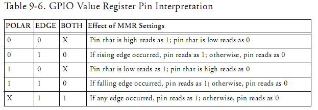
The state of the output is reflected on the associated pin only if the function enable bit in the PORTx_FER register is cleared.
- BF52x学习
- 学习
- 学习
- 学习
- 学习
- 学习
- 学习
- 学习
- 学习
- 学习
- 学习
- 学习
- 学习
- 学习
- 学习
- 学习
- 学习
- 学习
- Visual Studio预览版完成 或于下周发布
- ASP目录遍历
- 网络中的子网划分
- Delphi DBGridEh标题栏的制作(复杂标题栏、标题栏显示图片、按点标题栏进行排序)
- Eclipse常用插件在线安装和离线安装方式(不断更新中。。。)
- BF52x学习
- 更新内容:关于Windows Azure技术内容搜索的新页面可用
- Scrum
- CONCAT_WS函数
- ASP遍历数据库
- JSON的使用方法
- Web浏览器大比拼
- visual studio快捷键
- device 与device_driver之间的绑定