PCI规范学习笔记
来源:互联网 发布:淘宝会员店加盟 编辑:程序博客网 时间:2024/05/21 06:22
以前看过一段时间Cyclone FPGA控制PEX8111的程序,没看懂,最近又结合PCI规范重新看了一下。
PCI Speci rev2.3
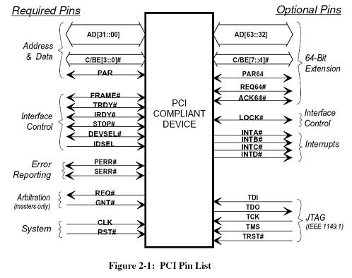
FRAME# is driven by the master to indicate the beginning and end of a
transaction.
IRDY# is driven by the master to indicate that it is ready to transfer data.
TRDY# is driven by the target to indicate that it is ready to transfer data.
IDSEL in Initialization Device Select is used as a chip select during
configuration read and write transactions.
STOP# s/t/s Stop indicates the current target is requesting the master to
stop the current transaction.
In all cases, data is only
transferred when IRDY# and TRDY# are both asserted on the same rising clock edge.
只有当IRDY# and TRDY#都有效时,数据才能传输。
3.2.2. Addressing
PCI targets (except host bus bridges) are required to implement Base Address register(s)
to request a range of addresses which can be used to provide access to internal registers
or functions (refer to Chapter 6 for more details). The configuration software uses the
Base Address register to determine how much space a device requires in a given address
space and then assigns (if possible) where in that space the device will reside.
BAR确定一个设备需要多少空间。
A
device may map its internal register into both Memory Space and optionally I/O Space
by using two Base Address registers, one for I/O and the other for Memory.
When a transaction is initiated on the interface, each potential target compares the
address with its Base Address register(s) to determine if it is the target of the current
transaction. If it is the target, the device asserts DEVSEL# to claim the access. For
more details about DEVSEL# generation, refer to Section 3.2.2.3.2. How a target
completes address decode in each address space is discussed in the following sections.
当一个交易初始后,每个潜在设备将自己的BAR与总线上的地址比较,来确定自己是不是当前交易的目标。
3.2.2.1. I/O Space Decoding
In the I/O Address Space, all 32 AD lines are used to provide a full byte address. The
master that initiates an I/O transaction is required to ensure that AD[1::0] indicate the
least significant valid byte for the transaction.
The byte enables indicate the size of the transfer and the affected bytes within the
DWORD and must be consistent with AD[1::0]. Table 3-1 lists the valid combinations
for AD[1::0] and the byte enables for the initial data phase.
3.2.2.2. Memory Space Decoding
In the Memory Address Space, the AD[31::02] bus provides a DWORD aligned
address. AD[1::0] are not part of the address decode. However, AD[1::0] indicate the
order in which the master is requesting the data to be transferred.
3.2.2.3. Configuration Space Decoding
In the
Configuration Address Space, each function is assigned a unique 256-byte space that is
accessed differently than I/O or Memory Address Spaces.
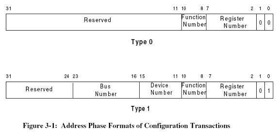
To support hierarchical PCI buses, two types of configuration transactions are used.
They have the formats illustrated in Figure 3-1, which shows the interpretation of AD
lines during the address phase of a configuration transaction.
Type 1 and Type 0 configuration transactions are differentiated by the values on
AD[1::0]. A Type 0 configuration transaction (when AD[1::0] = "00") is used to select
a device on the bus where the transaction is being run. A Type 1 configuration
transaction (when AD[1::0] = "01") is used to pass a configuration request to another
bus segment.
3.2.2.3.2. Software Generation of Configuration Transactions
Two DWORD I/O locations are used to generate configuration transactions for PC-AT
compatible systems. The first DWORD location (CF8h) references a read/write register
that is named CONFIG_ADDRESS. The second DWORD address (CFCh) references a
read/write register named CONFIG_DATA. The CONFIG_ADDRESS register is 32
bits with the format shown in Figure 3-2. Bit 31 is an enable flag for determining when
accesses to CONFIG_DATA are to be translated to configuration transactions on the PCI
bus. Bits 30 to 24 are reserved, read-only, and must return 0's when read. Bits 23
through 16 choose a specific PCI bus in the system. Bits 15 through 11 choose a specific
device on the bus. Bits 10 through 8 choose a specific function in a device (if the device
supports multiple functions). Bits 7 through 2 choose a DWORD in the device's
Configuration Space. Bits 1 and 0 are read-only and must return 0's when read.
Anytime a host bridge sees a full DWORD I/O write from the host to
CONFIG_ADDRESS, the bridge must latch the data into its CONFIG_ADDRESS
register. On full DWORD I/O reads to CONFIG_ADDRESS, the bridge must return the
data in CONFIG_ADDRESS.
配置空间的读写是通过读写两个IO端口实现的。
3.2.2.3.4. Selection of a Device’s Configuration Space
A single function device asserts DEVSEL# to claim a configuration transaction when:
a configuration command is decoded;
the device’s IDSEL is asserted; and
AD[1::0] is "00" (Type 0 Configuration Command) during the Address Phase.

有PCI系统的PC-AT系统,有2套总线系统,一套为PC-AT的总线,一套为PCI local bus的总线。
PC向IO端口CF8H和CFCH写数据,是通过PC-AT的总线写入CONFIG_ADDRESS和CONFIG_DATA的寄存器,然后PCI local bus根据CONFIG_ADDRESS和CONFIG_DATA的寄存器的值,产生PCI local bus的时序,诸如AD,CMB,FRAME等。
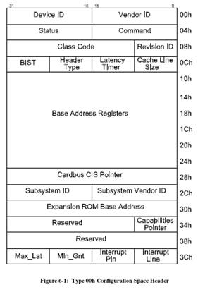
PCI配置空间有6个BAR,这些BAR既提供大小又提供数据类型信息。
if rst='0' then
basereg0<="11111111111111111111111100000001";
elsif rising_edge(clk) then
if (cfgwr='1' and base0='1' and wrsel='1') then
basereg0(31 downto 8)<=wrreg(31 downto 8);
basereg0(7 downto 0)<="00000001";
end if;
end if;
if rst='0' then
basereg1<="11111111110000000000000000000000";
elsif rising_edge(clk) then
if (cfgwr='1' and base1='1' and wrsel='1') then
basereg1(31 downto 22)<=wrreg(31 downto 22);
basereg1(21 downto 0)<="0000000000000000000000";
end if;
end if;
以上代码是PCIE开发板代码。
Base0的7-0位和Base1的21-0位是不能写的,PC机对其不能控制,第一位不是0的数的权值代表需要分配的大小。
所以,IO space要求分配的大小为2^8=256 byte,Memory space要求分配的大小为2^22=4M byte
6.2.5. Base Addresses
One of the most important functions for enabling superior configurability and ease of use
is the ability to relocate PCI devices in the address spaces.
可以把PCI设备地址重映射是PCI的一个优点之一。
Power-up software(BIOS?) needs to build a consistent address map before booting the machine to an operating system.
The number of upper bits that a device actually implements depends on how much of the
address space the device will respond to. A 32-bit register can be implemented to
support a single memory size that is a power of 2 from 16 bytes to 2 GB.
16 bytes to 2 GB.
2^4=16byte~2^31=1GB,因为Memory的0,1~2,3位有特殊意义。
A device that wants a 1 MB memory address space (using a 32-bit base address register) would build the top 12 bits of the address register, hardwiring the other bits to 0.
一个需要1MB内存地址空间的设备,需要将20~0bit,设为0,这样,可以提供2^21=1MB的空间。
hardwiring the other bits to 0.在一个有FPGA的设备中,就可以这样实现。
if rst='0' then
basereg0<="11111111111111111111111100000001";
elsif rising_edge(clk) then
if (cfgwr='1' and base0='1' and wrsel='1') then
basereg0(31 downto 8)<=wrreg(31 downto 8);
basereg0(7 downto 0)<="00000001";
end if;
end if;
Power-up software can determine how much address space the device requires by
writing a value of all 1's to the register and then reading the value back. The device will
return 0's in all don't-care address bits, effectively specifying the address space required.
Unimplemented Base Address registers are hardwired to zero.
加电软件(BIOS)可以确定设备需要多少地址空间,通过,向寄存器所有位写1,然后回读,回读数据中,第一个为1的位置的权值,即为设备请求的空间的大小,因为其他位,设备将其硬件置为0(FPGA实现)。
Devices that map control functions into I/O Space must not consume more than 256
bytes per I/O Base Address register. The upper 16 bits of the I/O Base Address register
may be hardwired to zero for devices intended for 16-bit I/O systems, such as PC
compatibles. However, a full 32-bit decode of I/O addresses must still be done.
PCI设备的每个IO BAR消耗的空间不得大于256 byte。
Implementation Note: Sizing a 32-bit Base Address Register
Example
Decode (I/O or memory) of a register is disabled via the command register before sizing
a Base Address register.
在设置BAR之前,IO和Memory空间的访问通过command寄存器被禁止了。
Software saves the original value of the Base Address register,
writes 0FFFFFFFFh to the register, then reads it back.
软件(BIOS?)先保存原来的BAR的值,然后对BAR寄存器写0FFFFFFFFh,再读回寄存器的值。
Size calculation can be done from
the 32-bit value read by first clearing encoding information bits (bit 0 for I/O, bits 0-3
for memory), inverting all 32 bits (logical NOT), then incrementing by 1. The resultant
32-bit value is the memory/I/O range size decoded by the register.
比如读回的是IO BAR(通过检查bit0),对编码信息清零(bit 0 for I/O, bits 0-3
for memory),取反,加1,即为IO空间请求的大小。然后软件为其分配地址空间,然后重新写回该BAR,而该BAR低n位硬件置为0,所以,自动进行了对齐。
Note that the upper
16 bits of the result is ignored if the Base Address register is for I/O and bits 16-31
returned zero upon read. The original value in the Base Address register is restored
before re-enabling decode in the command register of the device.
最小IO译码器,可以实现[31:2]的可写,PCI IO译码器的最小IO块为4。
最大IO译码器,可以实现[31:8]的可写,PCI IO译码器的最大IO块为256。
- PCI规范学习笔记
- PCI规范学习笔记(1)
- PCI规范学习笔记(2)
- PCI规范学习笔记,转载的
- PCI 学习笔记
- pci 学习笔记
- PCI 总线学习笔记
- pci设备学习笔记
- pci规范
- PCI规范
- PCI 总线学习笔记-PCI9054
- ACPI & PCI 学习笔记 1
- PCI学习笔记(zz)
- LDD3学习笔记(15):PCI驱动
- PCI MSI MSI-X学习笔记
- PCI总线学习笔记(一)
- PCIe学习笔记(1)---PCI相关
- 学习pci
- 别人的mfc笔记
- 二十二条
- Php解析土豆flv
- 字符转义
- oracle数据库建立链接
- PCI规范学习笔记
- mysql Connection.close() has already been called
- IDcard 验证代码----新身份证合法性验证
- 网络日志(2010.6.12)
- 要积分呢
- 处理团队的改变
- 谁有最新的 Adobe LiveCycle Designer
- 行列倒置 转换
- 智能卡的操作系统——COS