基于MTD的NANDFLASH设备驱动底层实现原理分析(六) .
来源:互联网 发布:java hadoop 下载文件 编辑:程序博客网 时间:2024/05/17 22:50
在Linux中NANDFLASH设备驱动是被注册成平台驱动的。我还是从函数的入口出发一步一个脚印的分析。突然间发现这些代码真的很经典
由于这一次CPU是S3C2440所以分析过程中会把其他的CPU去掉
七、mtd/nand/s3c2410.c函数的解析
1、函数中出现的几个结构体
struct s3c24xx_nand_mtd {
struct mtd_info mtd;/*用来表述MTD原始设备的结构*/
struct nand_chip chip;/*该结构体表示一个NAND芯片*/
//该结构定义在arch/arm/plat-s3c/include/plat/nand.h中,该结构体包含了一个或多个的NAND芯片的信息
struct s3c2410_nand_set *set;
struct s3c24xx_nand_info *info;
int scan_res;
};
/**CPU选型的枚举**/
enum s3c_cpu_type {
TYPE_S3C2410,
TYPE_S3C2440,
};
/**NANDFLASH控制器状态的结构**/
struct s3c24xx_nand_info {
/* mtd info */
//include/linux/mtd/nand.h硬件控制器结构
struct nand_hw_control controller;
struct s3c24xx_nand_mtd *mtds;
//NANDFLASH平台驱动结构
struct s3c2410_platform_nand *platform;
/* device info */
struct device *device;
struct resource *area;
struct clk *clk;
void __iomem *regs;
void __iomem *sel_reg;
int sel_bit;
int mtd_count;
unsigned long save_sel;
unsigned long clk_rate;
enum s3c_cpu_type cpu_type;
#ifdef CONFIG_CPU_FREQ
struct notifier_block freq_transition;
#endif
};
2、函数入口和出口
static struct platform_driver s3c24xx_nand_driver = {
.probe = s3c24xx_nand_probe,
.remove = s3c24xx_nand_remove,
.suspend = s3c24xx_nand_suspend,
.resume = s3c24xx_nand_resume,
.id_table = s3c24xx_driver_ids,
.driver = {
.name = "s3c24xx-nand",
.owner = THIS_MODULE,
},
};
static int __init s3c2410_nand_init(void)
{
printk("S3C24XX NAND Driver, (c) 2004 Simtec Electronics\n");
//这些已经没什么好解释的了。注册平台驱动
return platform_driver_register(&s3c24xx_nand_driver);
}
static void __exit s3c2410_nand_exit(void)
{
//当我们卸载内核模块的时候会呗调用 注销平台驱动
platform_driver_unregister(&s3c24xx_nand_driver);
}
module_init(s3c2410_nand_init);
module_exit(s3c2410_nand_exit);
MODULE_LICENSE("GPL");
MODULE_AUTHOR("Ben Dooks <ben@simtec.co.uk>");
MODULE_DESCRIPTION("S3C24XX MTD NAND driver");
3、NANDFLASH中的s3c24xx_nand_probe函数。
<随便提一句>可能我们都懂当我们向系统注册一个平台驱动的时候,会去遍历系统上的平台设备,找到能够与之相对应的平台设备。当找到可用的设备后该函数才会被调用<称之探测函数>对于外设来说驱动的本身应该是从这个探测函数真正开始的,那么它究竟有什么用呢?它到底做了什么事情,这可能是我们最关心的。在MTD/NAND的probe过程中,去用clk_enable打开Nand Flash控制器的clock时钟,用request_mem_region去申请驱动所需要的一些内存等相关资yuan然后,在 s3c2410_nand_inithw 中,去初始化硬件相关的部分,主要是关于时钟频率的计算,以及启用 Nand Flash 控制器,使得硬件初始化好了,后面才能正常工作。如果说把这个函数理解透了那么整个驱动起码是完成三分之二的工作了。在s3c2410.c中s3c24xx_nand_probe函数特别的长,所以一段一段的分析.
static int s3c24xx_nand_probe(struct platform_device *pdev)
{
/**从总线设备中取出平台设备的数据,我一直在思索最后这个结构会从哪里传进来呢?**如果你移植过Linux到你的开发板那么你一定会在你的板层文件中构建这样一个结构体请看下面步骤a)中的结构体*/
struct s3c2410_platform_nand *plat = to_nand_plat(pdev);
enum s3c_cpu_type cpu_type;
struct s3c2410_nand_info *info;
struct s3c2410_nand_mtd *nmtd;
struct s3c2410_nand_set *sets;
struct resource *res;
int err = 0;
int size;
int nr_sets;
int setno;
/*获取CPU类型*/
cpu_type = platform_get_device_id(pdev)->driver_data;
pr_debug("s3c2410_nand_probe(%p)\n", pdev);
/*为s3c2410_nand_info分配内存*/
info = kmalloc(sizeof(*info), GFP_KERNEL);
if (info == NULL) {
dev_err(&pdev->dev, "no memory for flash info\n");
err = -ENOMEM;
goto exit_error;
}
/**初始化s3c2410_nand_info**/
memset(info, 0, sizeof(*info));
/**将nand设备的数据信息传递到系统平台设备中去**/
platform_set_drvdata(pdev, info);
/**初始化自旋锁和等待队列**/
spin_lock_init(&info->controller.lock);
init_waitqueue_head(&info->controller.wq);
/* get the clock source and enable it */
info->clk = clk_get(&pdev->dev, "nand");
if (IS_ERR(info->clk)) {
dev_err(&pdev->dev, "failed to get clock\n");
err = -ENOENT;
goto exit_error;
}
clk_enable(info->clk);//使能时钟
/* allocate and map the resource */
/* currently we assume we have the one resource */
res = pdev->resource;
size = res->end - res->start + 1;
/**为资源申请IO内存**/
info->area = request_mem_region(res->start, size, pdev->name);
if (info->area == NULL) {
dev_err(&pdev->dev, "cannot reserve register region\n");
err = -ENOENT;
goto exit_error;
}
/*****这都是给info这个结构的成员变量赋值啊*没啥可说的,*/
info->device = &pdev->dev;
info->platform = plat;
info->regs = ioremap(res->start, size);
info->cpu_type = cpu_type;
if (info->regs == NULL) {
dev_err(&pdev->dev, "cannot reserve register region\n");
err = -EIO;
goto exit_error;
}
dev_dbg(&pdev->dev, "mapped registers at %p\n", info->regs);
/* initialise the hardware *//**解析c*/
/**初始化硬件**/
err = s3c2410_nand_inithw(info);
if (err != 0)
goto exit_error;
/*struct s3c2410_platform_nand 中包含了一个struct s3c2410_nand_set *sets
的成员变量 专门用来描述芯片信息的**/
sets = (plat != NULL) ? plat->sets : NULL;
nr_sets = (plat != NULL) ? plat->nr_sets : 1;
info->mtd_count = nr_sets;
/* allocate our information */
size = nr_sets * sizeof(*info->mtds);
info->mtds = kmalloc(size, GFP_KERNEL);
if (info->mtds == NULL) {
dev_err(&pdev->dev, "failed to allocate mtd storage\n");
err = -ENOMEM;
goto exit_error;
}
memset(info->mtds, 0, size);
/* initialise all possible chips */
nmtd = info->mtds;
for (setno = 0; setno < nr_sets; setno++, nmtd++) {
pr_debug("initialising set %d (%p, info %p)\n", setno, nmtd, info);
/**nand_chip结构的初始化**见下一遍分析d)**/
s3c2410_nand_init_chip(info, nmtd, sets);
/**读取芯片的ID**/
nmtd->scan_res = nand_scan_ident(&nmtd->mtd,
(sets) ? sets->nr_chips : 1);
if (nmtd->scan_res == 0) {
s3c2410_nand_update_chip(info, nmtd);
nand_scan_tail(&nmtd->mtd);
s3c2410_nand_add_partition(info, nmtd, sets);
}
if (sets != NULL)
sets++;
}
err = s3c2410_nand_cpufreq_register(info);
if (err < 0) {
dev_err(&pdev->dev, "failed to init cpufreq support\n");
goto exit_error;
}
if (allow_clk_stop(info)) {
dev_info(&pdev->dev, "clock idle support enabled\n");
clk_disable(info->clk);
}
pr_debug("initialised ok\n");
return 0;
exit_error:
s3c24xx_nand_remove(pdev);
if (err == 0)
err = -EINVAL;
return err;
}
我真不知道该怎么去分析这个程序。
a)分析该函数的第一行的代码我就迷茫了呵呵.看看下面这个结构体.你是否会发现什么
static struct s3c2410_platform_nand eilian240_nand_info = {
.tacls = 20,
.twrph0 = 60,
.twrph1 = 20,
.nr_sets = ARRAY_SIZE(eilian240_nand_sets),
.sets = eilian240_nand_sets,
.ignore_unset_ecc = 1,
};发现了吧这些芯片硬件信息是在我们移植的时候才传进去的<所以这就和目标板有关系了>
那么这些芯片信息又是怎样和系统里面的总线设备关联起来的呢?看下面这三句
info = kmalloc(sizeof(*info), GFP_KERNEL); 为info结构分配内存
memset(info, 0, sizeof(*info)); //初始化内存
platform_set_drvdata(pdev, info); //别小看这一句,功能可强大了,这些芯片信息就是通过它传递到总线设备里面去的,看下源代码你就明白了
b)关于时钟使能和平台设备驱动程序,想设备申请资源这是必须要做的事情,我解释不了,表达能力很有限哦。
c)硬件的初始化函数s3c2410_nand_inithw(info);其实就是在设置一些寄存器和时钟的频率,看看它是怎么实现的
static int s3c2410_nand_inithw(struct s3c2410_nand_info *info)
{
int ret;
ret = s3c2410_nand_setrate(info);
if (ret < 0)
return ret;
switch (info->cpu_type) {
case TYPE_S3C2410:
default:
break;
case TYPE_S3C2440:
case TYPE_S3C2412:
/* enable the controller and de-assert nFCE */
writel(S3C2440_NFCONT_ENABLE, info->regs + S3C2440_NFCONT);
}
return 0;
}
static int s3c2410_nand_setrate(struct s3c2410_nand_info *info)
{
struct s3c2410_platform_nand *plat = info->platform;
int tacls_max = (info->cpu_type == TYPE_S3C2412) ? 8 : 4;
int tacls, twrph0, twrph1;
/**获取时钟频率**/
unsigned long clkrate = clk_get_rate(info->clk);//这个时钟我们在之前已经获取了吧
unsigned long uninitialized_var(set), cfg, uninitialized_var(mask);//这其实都是一些宏,看看源代码就知道了 unsigned long flags;
/* calculate the timing information for the controller */
info->clk_rate = clkrate;
clkrate /= 1000; /* turn clock into kHz for ease of use */
if (plat != NULL) {
tacls = s3c_nand_calc_rate(plat->tacls, clkrate, tacls_max);
twrph0 = s3c_nand_calc_rate(plat->twrph0, clkrate, 8);
twrph1 = s3c_nand_calc_rate(plat->twrph1, clkrate, 8);
} else {
/* default timings */
tacls = tacls_max;
twrph0 = 8;
twrph1 = 8;
}
if (tacls < 0 || twrph0 < 0 || twrph1 < 0) {
dev_err(info->device, "cannot get suitable timings\n");
return -EINVAL;
}
dev_info(info->device, "Tacls=%d, %dns Twrph0=%d %dns, Twrph1=%d %dns\n",
tacls, to_ns(tacls, clkrate), twrph0, to_ns(twrph0, clkrate), twrph1, to_ns(twrph1, clkrate));
switch (info->cpu_type) {
。。。。。。。
case TYPE_S3C2440:
case TYPE_S3C2412:
mask = (S3C2440_NFCONF_TACLS(tacls_max - 1) |
S3C2440_NFCONF_TWRPH0(7) |
S3C2440_NFCONF_TWRPH1(7));
set = S3C2440_NFCONF_TACLS(tacls - 1);
set |= S3C2440_NFCONF_TWRPH0(twrph0 - 1);
set |= S3C2440_NFCONF_TWRPH1(twrph1 - 1);
break;
default:
BUG();
}
local_irq_save(flags);
cfg = readl(info->regs + S3C2410_NFCONF);
cfg &= ~mask;
cfg |= set;
writel(cfg, info->regs + S3C2410_NFCONF);
local_irq_restore(flags);
dev_dbg(info->device, "NF_CONF is 0x%lx\n", cfg);
return 0;
}
在分析这几段代码的时候我为Nandflash存储的时序纠结了好久,看看下面这个图,S3C2440数据手册上的
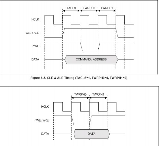
TACLS:当CLE/ALE使能后再过多长的时间nWe才有效/* time for active CLE/ALE to nWE/nOE */
TWRPH0:nWE/nRE的有效时间的长度 /* active time for nWE/nOE */
TWRPH1:nWE/nRE无效开始到CLE/ALE也无效的时间的长度 /* time for release CLE/ALE from nWE/nOE inactive */
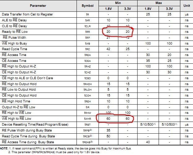
不知道是不是这样的....如果分析错了有大神看到请指出。在k9f2g08上有这样一个表
所以有a中的:
.tacls = 20,
.twrph0 = 60,
.twrph1 = 20, 不过到这个地方我还是有一点点的迷惑不知道是我的数据手册错了还是什么,随便找了一个时序看了看时间不对啊。。。。。
int tacls_max = (info->cpu_type == TYPE_S3C2412) ? 8 : 4;//这一句先看看下面这个表2<对下面分析还要用到的>

红色标注的部分不是明明是0---3么 怎么这里设置的4呢?别急继续往下看。。
tacls ,twrph0,twrph1它是怎么进行转换的呢
static int s3c_nand_calc_rate(int wanted, unsigned long clk, int max)
{
int result;
/**[(wanted * clk)+NS_IN_KHZ)-1]/NS_IN_KHZ */
result = DIV_ROUND_UP((wanted * clk), NS_IN_KHZ);
/** #define NS_IN_KHZ 1000000 //原本单位是HZ现在转换成KHZ**/
pr_debug("result %d from %ld, %d\n", result, clk, wanted);
if (result > max) {
printk("%d ns is too big for current clock rate %ld\n", wanted, clk);
return -1;
}
if (result < 1)
result = 1;
return result;
}
现在再往上看那段if(plat != NULL){。。。。。。。。}或许明白了
再返回 int s3c2410_nand_setrate(struct s3c2410_nand_info *info)中下面这段代码
switch (info->cpu_type) {
。。。。。。。
case TYPE_S3C2440:
case TYPE_S3C2412:
/**好了现在来了个tacls_max - 1或许就明白了上面为何是4而不是3了。这些代码都是在给NANDFLASH配置寄存器的相应的位赋值,不过还没有写进去。后面有写入的操作的。*/
mask = (S3C2440_NFCONF_TACLS(tacls_max - 1) |
S3C2440_NFCONF_TWRPH0(7) |
S3C2440_NFCONF_TWRPH1(7));
set = S3C2440_NFCONF_TACLS(tacls - 1);
set |= S3C2440_NFCONF_TWRPH0(twrph0 - 1);
set |= S3C2440_NFCONF_TWRPH1(twrph1 - 1);
break;
。。。。。。。。。。。。。
/**将这些数据写进寄存器中去*/
cfg = readl(info->regs + S3C2410_NFCONF);
cfg &= ~mask;
cfg |= set;
writel(cfg, info->regs + S3C2410_NFCONF);
再返回static int s3c2410_nand_inithw(struct s3c2410_nand_info *info)有这么一断代码
。。。。。。。。
case TYPE_S3C2440:
case TYPE_S3C2412:
/* enable the controller and de-assert nFCE */
/*****使能NANDFLASH控制寄存器******/
writel(S3C2440_NFCONT_ENABLE, info->regs + S3C2440_NFCONT);
}
/***********到这里为止这个硬件的初始化工作就结束了***************************************************/
上面基本的硬件初始化完后应该是要初始化nand_chip实例了,并运行nand_scan()扫描NAND设备了,最后添加板文件中的分区表。nand_chip是NANDFLASH驱动的核心结构上一遍文章已经分析过了。还是放到下一遍文章吧
http://blog.csdn.net/bingqingsuimeng/article/details/7968359
- 基于MTD的NANDFLASH设备驱动底层实现原理分析
- 基于MTD的NANDFLASH设备驱动底层实现原理分析 .
- 基于MTD的NANDFLASH设备驱动底层实现原理分析(六)
- 基于MTD的NANDFLASH设备驱动底层实现原理分析(六)
- 基于MTD的NANDFLASH设备驱动底层实现原理分析(六) .
- 基于MTD的NANDFLASH设备驱动底层实现原理分析(六)
- 基于MTD的NANDFLASH设备驱动底层实现原理分析(六)
- 基于MTD的NANDFLASH设备驱动底层实现原理分析(一)
- 基于MTD的NANDFLASH设备驱动底层实现原理分析(二)
- 基于MTD的NANDFLASH设备驱动底层实现原理分析(三)
- 基于MTD的NANDFLASH设备驱动底层实现原理分析(四)
- 基于MTD的NANDFLASH设备驱动底层实现原理分析(五)
- 基于MTD的NANDFLASH设备驱动底层实现原理分析(七)
- 基于MTD的NANDFLASH设备驱动底层实现原理分析(一)
- 基于MTD的NANDFLASH设备驱动底层实现原理分析(二)
- 基于MTD的NANDFLASH设备驱动底层实现原理分析(三)
- 基于MTD的NANDFLASH设备驱动底层实现原理分析(四)
- 基于MTD的NANDFLASH设备驱动底层实现原理分析(五)
- 技术团队新官上任之基层篇
- 小议SEO做网站关键字优化
- 基于MTD的NANDFLASH设备驱动底层实现原理分析(七) .
- 如何关闭80端口(8080端口同样原理),如何查找哪些端口在使用中
- 值得推荐的经典电影
- 基于MTD的NANDFLASH设备驱动底层实现原理分析(六) .
- 如何特意制造栈缓冲区溢出?(x86 & ARM)
- 中缀表达式转化成前缀表达式和后缀表达式
- iOS 宏编译debug调试
- UIPopoverController的使用,看着很牛逼的样子
- linux 常用的命令
- 基于MTD的NANDFLASH设备驱动底层实现原理分析(五) .
- linux不能使用sudo命令解决方案
- 基于MTD的NANDFLASH设备驱动底层实现原理分析(四) .