PCI Express
来源:互联网 发布:毕加索美工钢笔推荐 编辑:程序博客网 时间:2024/05/29 17:58
PCI Express (Peripheral Component Interconnect Express), officially abbreviated as PCIe, is a high-speed serialcomputer expansion bus standard, designed to replace the older PCI, PCI-X, and AGP bus standards. PCIe has numerous improvements over the older standards, including higher maximum system bus throughput, lower I/O pin count and smaller physical footprint, better performance scaling for bus devices, a more detailed error detection and reporting mechanism (Advanced Error Reporting, AER[1]), and native hot-plug functionality. More recent revisions of the PCIe standard provide hardware support for I/O virtualization.
The PCI Express electrical interface is also used in a variety of other standards, most notably in ExpressCard as alaptop expansion card interface, and in SATA Express as a computer storage interface.
Format specifications are maintained and developed by the PCI-SIG (PCI Special Interest Group), a group of more than 900 companies that also maintain the conventional PCI specifications. PCIe 3.0 is the latest standard for expansion cards that are in production and available on mainstream personal computers.[2][3]
Contents
[hide]- 1Architecture
- 1.1Interconnect
- 1.2Lane
- 1.3Serial bus
- 2Form factors
- 2.1PCI Express (standard)
- 2.1.1Pinout
- 2.1.2Power
- 2.2PCI Express Mini Card
- 2.2.1Physical dimensions
- 2.2.2Electrical interface
- 2.3Mini-SATA (mSATA) variant
- 2.4PCI Express External Cabling
- 2.5Derivative forms
- 2.1PCI Express (standard)
- 3History and revisions
- 3.1PCI Express 1.0a
- 3.2PCI Express 1.1
- 3.3PCI Express 2.0
- 3.4PCI Express 2.1
- 3.5PCI Express 3.0
- 3.6PCI Express 3.1
- 3.7PCI Express 4.0
- 3.8Extensions and future directions
- 4Hardware protocol summary
- 4.1Physical layer
- 4.1.1Data transmission
- 4.2Data link layer
- 4.3Transaction layer
- 4.1Physical layer
- 5Applications
- 5.1External GPUs
- 5.2Storage devices
- 5.3Cluster interconnect
- 6Competing protocols
- 7See also
- 8Notes
- 9References
- 10Further reading
- 11External links
Architecture[edit]
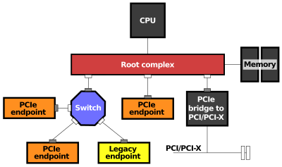

Conceptually, the PCI Express bus is a high-speed serial replacement of the older PCI/PCI-X bus.[5]One of the key differences between the PCI Express bus and the older PCI is the bus topology; PCI uses a shared parallel bus architecture, in which the PCI host and all devices share a common set of address, data and control lines. In contrast, PCI Express is based on point-to-point topology, with separate serial links connecting every device to the root complex (host). Due to its shared bus topology, access to the older PCI bus is arbitrated (in the case of multiple masters), and limited to one master at a time, in a single direction. Furthermore, the older PCI clocking scheme limits the bus clock to the slowest peripheral on the bus (regardless of the devices involved in the bus transaction). In contrast, a PCI Express bus link supports full-duplex communication between any two endpoints, with no inherent limitation on concurrent access across multiple endpoints.
In terms of bus protocol, PCI Express communication is encapsulated in packets. The work of packetizing and de-packetizing data and status-message traffic is handled by the transaction layer of the PCI Express port (described later). Radical differences in electrical signaling and bus protocol require the use of a different mechanical form factor and expansion connectors (and thus, new motherboards and new adapter boards); PCI slots and PCI Express slots are not interchangeable. At the software level, PCI Express preserves backward compatibility with PCI; legacy PCI system software can detect and configure newer PCI Express devices without explicit support for the PCI Express standard, though new PCI Express features are inaccessible.
The PCI Express link between two devices can consist of anywhere from one to 32 lanes. In a multi-lane link, the packet data is striped across lanes, and peak data throughput scales with the overall link width. The lane count is automatically negotiated during device initialization, and can be restricted by either endpoint. For example, a single-lane PCI Express (×1) card can be inserted into a multi-lane slot (×4, ×8, etc.), and the initialization cycle auto-negotiates the highest mutually supported lane count. The link can dynamically down-configure itself to use fewer lanes, providing a failure tolerance in case bad or unreliable lanes are present. The PCI Express standard defines slots and connectors for multiple widths: ×1, ×4, ×8, ×12, ×16 and ×32.[4]:4,5 This allows the PCI Express bus to serve both cost-sensitive applications where high throughput is not needed, as well as performance-critical applications such as 3D graphics, networking (10 Gigabit Ethernet or multiport Gigabit Ethernet), and enterprise storage (SAS or Fibre Channel).
As a point of reference, a PCI-X (133 MHz 64-bit) device and a PCI Express 1.0 device using four lanes (×4) have roughly the same peak single-direction transfer rate of 1064 MB/s. The PCI Express bus has the potential to perform better than the PCI-X bus in cases where multiple devices are transferring data simultaneously, or if communication with the PCI Express peripheral is bidirectional.
Interconnect[edit]

PCI Express devices communicate via a logical connection called an interconnect[6] or link. A link is a point-to-point communication channel between two PCI Express ports allowing both of them to send and receive ordinary PCI requests (configuration, I/O or memory read/write) and interrupts(INTx, MSI or MSI-X). At the physical level, a link is composed of one or more lanes.[6] Low-speed peripherals (such as an 802.11 Wi-Fi card) use a single-lane (×1) link, while a graphics adapter typically uses a much wider and faster 16-lane link.
Lane[edit]
A lane is composed of two differential signaling pairs, with one pair for receiving data and the other for transmitting. Thus, each lane is composed of four wires or signal traces. Conceptually, each lane is used as a full-duplex byte stream, transporting data packets in eight-bit "byte" format simultaneously in both directions between endpoints of a link.[7] Physical PCI Express links may contain from one to 32 lanes, more precisely 1, 2, 4, 8, 12, 16 or 32 lanes.[4]:4,5[6] Lane counts are written with an "×" prefix (for example, "×8" represents an eight-lane card or slot), with ×16 being the largest size in common use.[8]
Serial bus[edit]
The bonded serial bus architecture was chosen over the traditional parallel bus due to inherent limitations of the latter, including half-duplex operation, excess signal count, and inherently lower bandwidth due to timing skew. Timing skew results from separate electrical signals within a parallel interface traveling through conductors of different lengths, on potentially different printed circuit board (PCB) layers, and at possibly different signal velocities. Despite being transmitted simultaneously as a single word, signals on a parallel interface have different travel duration and arrive at their destinations at different times. When the interface clock period is shorter than the largest time difference between signal arrivals, recovery of the transmitted word is no longer possible. Since timing skew over a parallel bus can amount to a few nanoseconds, the resulting bandwidth limitation is in the range of hundreds of megahertz.
A serial interface does not exhibit timing skew because there is only one differential signal in each direction within each lane, and there is no external clock signal since clocking information is embedded within the serial signal itself. As such, typical bandwidth limitations on serial signals are in the multi-gigahertz range. PCI Express is one example of the general trend toward replacing parallel buses with serial interconnects; other examples include Serial ATA(SATA), USB, Serial Attached SCSI (SAS), FireWire (IEEE 1394), and RapidIO. In digital video, examples in common use are DVI, HDMI and DisplayPort.
Multichannel serial design increases flexibility with its ability to allocate fewer lanes for slower devices.
Form factors[edit]
PCI Express (standard)[edit]

A PCI Express card fits into a slot of its physical size or larger (with ×16 as the largest used), but may not fit into a smaller PCI Express slot; for example, a ×16 card may not fit into a ×4 or ×8 slot. Some slots use open-ended sockets to permit physically longer cards and negotiate the best available electrical and logical connection.
The number of lanes actually connected to a slot may also be fewer than the number supported by the physical slot size. An example is a ×16 slot that runs at ×4, which will accept any ×1, ×2, ×4, ×8 or ×16 card, but provides only four lanes. Its specification may read as "×16 (×4 mode)", while "×size @ ×speed" notation ("×16 @ ×4") is also common. The advantage is that such slots can accommodate a larger range of PCI Express cards without requiring motherboard hardware to support the full transfer rate.
The cards themselves are designed and manufactured in various sizes. For example, solid-state drives(SSDs) that come in the form of PCI Express cards often use HHHL (half height, half length) and FHHL(full height, half length) to describe the physical dimensions of the card.[9][10]
Pinout[edit]
The following table identifies the conductors on each side of the edge connector on a PCI Express card. The solder side of the printed circuit board (PCB) is the A side, and the component side is the B side.[11] PRSNT1# and PRSNT2# pins must be slightly shorter than the rest, to ensure that a hot-plugged card is fully inserted. The WAKE# pin uses full voltage to wake the computer, but must be pulled high from the standby power to indicate that the card is wake capable.[12]
Power[edit]

All sizes of ×4 and ×8 PCI Express cards are allowed a maximum power consumption of 25 W. All ×1 cards are initially 10 W; full-height cards may configure themselves as 'high-power' to reach 25 W, while half-height ×1 cards are fixed at 10 W. All sizes of ×16 cards are initially 25 W; like ×1 cards, half-height cards are limited to this number while full-height cards may increase their power after configuration. They can use up to 75 W (3.3 V × 3 A + 12 V × 5.5 A), though the specification demands that the higher-power configuration be used for graphics cards only, while cards of other purposes are to remain at 25 W.[12][13]
Optional connectors add 75 W (6-pin) or 150 W (8-pin) power for up to 300 W total (2×75 W + 1×150 W). Some cards are using two 8-pin connectors, but this has not been standardized yet, therefore such cards must not carry the official PCI Express logo. This configuration would allow 375 W total (1×75 W + 2×150 W) and will likely be standardized by PCI-SIG with the PCI Express 4.0 standard. The 8-pin PCI Express connector could be mistaken with the EPS12V connector, which is mainly used for powering SMP and multi-core systems.
6-pin power connector (75 W)[14] 8-pin power connector (150 W)[15][16][17]- When a 6-pin connector is plugged into an 8-pin receptacle the card is notified by a missing Sense1 that it may only use up to 75 W.
PCI Express Mini Card[edit]


PCI Express Mini Card (also known as Mini PCI Express, Mini PCIe, Mini PCI-E, mPCIe, and PEM), based on PCI Express, is a replacement for the Mini PCI form factor. It is developed by the PCI-SIG. The host device supports both PCI Express and USB 2.0 connectivity, and each card may use either standard. Most laptop computers built after 2005 use PCI Express for expansion cards; however, as of 2015, many vendors are moving toward using the newer M.2 form factor for this purpose.
Due to different dimensions, PCI Express Mini Cards are not physically compatible with standard full-size PCI Express slots; however, passive adapters exist that allow them to be used in full-size slots.[18]
Physical dimensions[edit]
Dimensions of PCI Express Mini Cards are 30 × 50.95 mm (width × length) for a Full Mini Card. There is a 52-pin edge connector, consisting of two staggered rows on a 0.8 mm pitch. Each row has eight contacts, a gap equivalent to four contacts, then a further 18 contacts. Boards have a thickness of 1.0 mm, excluding the components. A "Half Mini Card" (sometimes abbreviated as HMC) is also specified, having approximately half the physical length of 26.8 mm.
Electrical interface[edit]
PCI Express Mini Card edge connectors provide multiple connections and buses:
- PCI Express ×1
- USB 2.0
- SMBus
- Wires to diagnostics LEDs for wireless network (i.e., Wi-Fi) status on computer's chassis
- SIM card for GSM and WCDMA applications. (UIM signals on spec)
- Future extension for another PCIe lane
- 1.5 V and 3.3 V power
Mini-SATA (mSATA) variant[edit]
Despite sharing the Mini PCI Express form factor, an mSATA slot is not necessarily electrically compatible with Mini PCI Express. For this reason, only certain notebooks are compatible with mSATA drives. Most compatible systems are based on Intel's Sandy Bridge processor architecture, using the Huron River platform. Notebooks like Lenovo's ThinkPad T, W and X series, released in March–April 2011, have support for an mSATA SSD card in their WWAN card slot. The ThinkPad Edge E220s/E420s, and the Lenovo IdeaPad Y460/Y560 also support mSATA.[19]
Some notebooks (notably the Asus Eee PC, the Apple MacBook Air, and the Dell mini9 and mini10) use a variant of the PCI Express Mini Card as an SSD. This variant uses the reserved and several non-reserved pins to implement SATA and IDE interface passthrough, keeping only USB, ground lines, and sometimes the core PCIe 1x bus intact.[20] This makes the "miniPCIe" flash and solid-state drives sold for netbooks largely incompatible with true PCI Express Mini implementations.
Also, the typical Asus miniPCIe SSD is 71 mm long, causing the Dell 51 mm model to often be (incorrectly) referred to as half length. A true 51 mm Mini PCIe SSD was announced in 2009, with two stacked PCB layers that allow for higher storage capacity. The announced design preserves the PCIe interface, making it compatible with the standard mini PCIe slot. No working product has yet been developed.
Intel has numerous desktop boards with the PCIe ×1 Mini-Card slot which typically do not support mSATA SSD. A list of desktop boards that natively support mSATA in the PCIe ×1 Mini-Card slot (typically multiplexed with a SATA port) is provided on the Intel Support site.[21]
PCI Express External Cabling[edit]
PCI Express External Cabling (also known as External PCI Express, Cabled PCI Express, or ePCIe) specifications were released by the PCI-SIG in February 2007.[22][23]
Standard cables and connectors have been defined for ×1, ×4, ×8, and ×16 link widths, with a transfer rate of 250 MB/s per lane. The PCI-SIG also expects the norm will evolve to reach 500 MB/s, as in PCI Express 2.0. The maximum cable length remains undetermined. An example of the uses of Cabled PCI Express is a metal enclosure, containing a number of PCI slots and PCI-to-ePCIe adapter circuitry. This device would not be possible had it not been for the ePCIe spec.
Derivative forms[edit]
There are several other expansion card types derived from PCIe. These include:
- Low-height card
- ExpressCard: successor to the PC Card form factor (with ×1 PCIe and USB 2.0; hot-pluggable)
- PCI Express ExpressModule: a hot-pluggable modular form factor defined for servers and workstations
- XQD card: a PCI Express-based flash card standard by the CompactFlash Association
- XMC: similar to the CMC/PMC form factor (VITA 42.3)
- AdvancedTCA: a complement to CompactPCI for larger applications; supports serial based backplane topologies
- AMC: a complement to the AdvancedTCA specification; supports processor and I/O modules on ATCA boards (×1, ×2, ×4 or ×8 PCIe).
- FeaturePak: a tiny expansion card format (43 × 65 mm) for embedded and small form factor applications; it implements two ×1 PCIe links on a high-density connector along with USB, I2C, and up to 100 points of I/O.
- Universal IO: A variant from Super Micro Computer Inc designed for use in low-profile rack-mounted chassis.[24] It has the connector bracket reversed so it cannot fit in a normal PCI Express socket, but it is pin-compatible and may be inserted if the bracket is removed.
- Thunderbolt: A variant from Intel that combines DisplayPort and PCIe protocols in a form factor compatible with Mini DisplayPort. Thunderbolt 3.0 also combines USB 3.1 and uses the USB Type-C form factor as opposed to Mini DisplayPort
- Serial Digital Video Out: some 9xx series Intel chipsets allow for adding another output for the integrated video into a PCIe slot (mostly dedicated and 16 lanes)
- M.2 (formerly known as NGFF)
- M-PCIe brings PCIe 3.0 to mobile devices (such as tablets and smartphones), over the M-PHY physical layer.[25][26]
- U.2 (formerly known as SFF-8639)
History and revisions[edit]
While in early development, PCIe was initially referred to as HSI (for High Speed Interconnect), and underwent a name change to 3GIO (for 3rd Generation I/O) before finally settling on its PCI-SIG name PCI Express. A technical working group named the Arapaho Work Group (AWG) drew up the standard. For initial drafts, the AWG consisted only of Intel engineers; subsequently the AWG expanded to include industry partners.
PCI Express is a technology under constant development and improvement.
As of 2013, PCI Express version 4 has been drafted with final specifications expected in 2017.[27] Synopsys showned on the 2016 Intel Developer Forum a system running on PCIe 4.0, while Mellanox had the adequate network card.[28]
version
PCI Express 1.0a[edit]
In 2003, PCI-SIG introduced PCIe 1.0a, with a per-lane data rate of 250 MB/s and a transfer rate of 2.5 gigatransfers per second (GT/s). Transfer rate is expressed in transfers per second instead of bits per second because the number of transfers includes the overhead bits, which do not provide additional throughput;[30] PCIe 1.x uses an 8b/10b encoding scheme, resulting in a 20% (= 2/10) overhead on the raw channel bandwidth.[31]
PCI Express 1.1[edit]
In 2005, PCI-SIG[32] introduced PCIe 1.1. This updated specification includes clarifications and several improvements, but is fully compatible with PCI Express 1.0a. No changes were made to the data rate.
PCI Express 2.0[edit]

PCI-SIG announced the availability of the PCI Express Base 2.0 specification on 15 January 2007.[33] The PCIe 2.0 standard doubles the transfer rate compared with PCIe 1.0 to 5 GT/s and the per-lane throughput rises from 250 MB/s to 500 MB/s. Consequently, a 32-lane PCIe connector (×32) can support an aggregate throughput of up to 16 GB/s.
PCIe 2.0 motherboard slots are fully backward compatible with PCIe v1.x cards. PCIe 2.0 cards are also generally backward compatible with PCIe 1.x motherboards, using the available bandwidth of PCI Express 1.1. Overall, graphic cards or motherboards designed for v2.0 will work with the other being v1.1 or v1.0a.
The PCI-SIG also said that PCIe 2.0 features improvements to the point-to-point data transfer protocol and its software architecture.[34]
Intel's first PCIe 2.0 capable chipset was the X38 and boards began to ship from various vendors (Abit, Asus, Gigabyte) as of October 21, 2007.[35] AMD started supporting PCIe 2.0 with its AMD 700 chipset series and nVidia started with theMCP72.[36] All of Intel's prior chipsets, including the Intel P35 chipset, supported PCIe 1.1 or 1.0a.[37]
Like 1.x, PCIe 2.0 uses an 8b/10b encoding scheme, therefore delivering, per-lane, an effective 4 Gbit/s max transfer rate from its 5 GT/s raw data rate.
PCI Express 2.1[edit]
PCI Express 2.1 (with its specification dated March 4, 2009) supports a large proportion of the management, support, and troubleshooting systems planned for full implementation in PCI Express 3.0. However, the speed is the same as PCI Express 2.0. Unfortunately, the increase in power from the slot breaks backward compatibility between PCI Express 2.1 cards and some older motherboards with 1.0/1.0a, but most motherboards with PCI Express 1.1 connectors are provided with a BIOS update by their manufacturers through utilities to support backward compatibility of cards with PCIe 2.1.
PCI Express 3.0[edit]
PCI Express 3.0 Base specification revision 3.0 was made available in November 2010, after multiple delays. In August 2007, PCI-SIG announced that PCI Express 3.0 would carry a bit rate of 8 gigatransfers per second (GT/s), and that it would be backward compatible with existing PCI Express implementations. At that time, it was also announced that the final specification for PCI Express 3.0 would be delayed until Q2 2010.[38] New features for the PCI Express 3.0 specification include a number of optimizations for enhanced signaling and data integrity, including transmitter and receiver equalization, PLL improvements, clock data recovery, and channel enhancements for currently supported topologies.[39]
Following a six-month technical analysis of the feasibility of scaling the PCI Express interconnect bandwidth, PCI-SIG's analysis found that 8 gigatransfers per second can be manufactured in mainstream silicon process technology, and can be deployed with existing low-cost materials and infrastructure, while maintaining full compatibility (with negligible impact) to the PCI Express protocol stack.
PCI Express 3.0 upgrades the encoding scheme to 128b/130b from the previous 8b/10b encoding, reducing the bandwidth overhead from 20% of PCI Express 2.0 to approximately 1.54% (= 2/130). This is achieved by a technique called "scrambling" that applies a known binary polynomial to a data stream in a feedback topology. Because the scrambling polynomial is known, the data can be recovered by running it through a feedback topology using the inverse polynomial. PCI Express 3.0's 8 GT/s bit rate effectively delivers 985 MB/s per lane, practically doubling the lane bandwidth relative to PCI Express 2.0.[29]
On November 18, 2010, the PCI Special Interest Group officially published the finalized PCI Express 3.0 specification to its members to build devices based on this new version of PCI Express.[40]
PCI Express 3.1[edit]
In September 2013, PCI Express 3.1 specification was announced to be released in late 2013 or early 2014, consolidating various improvements to the published PCI Express 3.0 specification in three areas: power management, performance and functionality.[26][41] It was released in November 2014.[42]
PCI Express 4.0[edit]
On November 29, 2011, PCI-SIG announced PCI Express 4.0,[43] providing a 16 GT/s bit rate that doubles the bandwidth provided by PCI Express 3.0, while maintaining backward and forward compatibility in both software support and used mechanical interface. Additionally, active and idle power optimizations are to be investigated. Final specifications are expected to be released in 2017.[44][45] Included in the specifications will be an increase in power to the slot from 75W to between 300-500W which would be enough to power a current GeForce 10 series (1080 and Titan) without the need for extra power feeds. [46]
On the Intel Developer Forum, Synopsys presented a test machine running PCIe 4.0. Their IP has been licensed to several firms plannning to present their chips and products at the end of 2016.[28]
Extensions and future directions[edit]
Some vendors offer PCIe over fiber products,[47][48][49] but these generally find use only in specific cases where transparent PCIe bridging is preferable to using a more mainstream standard (such as InfiniBand or Ethernet) that may require additional software to support it; current implementations focus on distance rather than raw bandwidth and typically do not implement a full ×16 link.
Thunderbolt was co-developed by Intel and Apple as a general-purpose high speed interface combining a ×4 PCIe link with DisplayPort and was originally intended to be an all-fiber interface, but due to early difficulties in creating a consumer-friendly fiber interconnect, most early implementations are hybrid copper-fiber systems. A notable exception, the Sony VAIO Z VPC-Z2, uses a nonstandard USB port with an optical component to connect to an outboard PCIe display adapter. Apple has been the primary driver of Thunderbolt adoption through 2011, though several other vendors[50] have announced new products and systems featuring Thunderbolt.
Mobile PCIe specification (abbreviated to M-PCIe) allows PCI Express architecture to operate over the MIPI Alliance's M-PHY physical layer technology. Building on top of already existing widespread adoption of M-PHY and its low-power design, Mobile PCIe allows PCI Express to be used in tablets and smartphones.[51]
OCuLink (standing for "optical-copper link") is an extension for the "cable version of PCI Express", acting as a competitor to version 3 of the Thunderbolt interface. Version 1.0 of OCuLink, to be released in fall 2015, supports up to four PCIe 3.0 lanes (8 GT/s, 3.9 GB/s) over copper cabling; a fiber optic version may appear in the future.[26][52]
Hardware protocol summary[edit]
The PCIe link is built around dedicated unidirectional couples of serial (1-bit), point-to-point connections known as lanes. This is in sharp contrast to the earlier PCI connection, which is a bus-based system where all the devices share the same bidirectional, 32-bit or 64-bit parallel bus.
PCI Express is a layered protocol, consisting of a transaction layer, a data link layer, and a physical layer. The Data Link Layer is subdivided to include amedia access control (MAC) sublayer. The Physical Layer is subdivided into logical and electrical sublayers. The Physical logical-sublayer contains a physical coding sublayer (PCS). The terms are borrowed from the IEEE 802 networking protocol model.
Physical layer[edit]
The PCIe Physical Layer (PHY, PCIEPHY, PCI Express PHY, or PCIe PHY) specification is divided into two sub-layers, corresponding to electrical and logical specifications. The logical sublayer is sometimes further divided into a MAC sublayer and a PCS, although this division is not formally part of the PCIe specification. A specification published by Intel, the PHY Interface for PCI Express (PIPE),[54] defines the MAC/PCS functional partitioning and the interface between these two sub-layers. The PIPE specification also identifies the physical media attachment (PMA) layer, which includes theserializer/deserializer (SerDes) and other analog circuitry; however, since SerDes implementations vary greatly among ASIC vendors, PIPE does not specify an interface between the PCS and PMA.
At the electrical level, each lane consists of two unidirectional LVDS pairs operating at 2.5, 5, 8 or 16 Gbit/s, depending on the negotiated capabilities. Transmit and receive are separate differential pairs, for a total of four data wires per lane.
A connection between any two PCIe devices is known as a link, and is built up from a collection of one or more lanes. All devices must minimally support single-lane (×1) link. Devices may optionally support wider links composed of 2, 4, 8, 12, 16, or 32 lanes. This allows for very good compatibility in two ways:
- A PCIe card physically fits (and works correctly) in any slot that is at least as large as it is (e.g., an ×1 sized card will work in any sized slot);
- A slot of a large physical size (e.g., ×16) can be wired electrically with fewer lanes (e.g., ×1, ×4, ×8, or ×12) as long as it provides the ground connections required by the larger physical slot size.
In both cases, PCIe negotiates the highest mutually supported number of lanes. Many graphics cards, motherboards and BIOSversions are verified to support ×1, ×4, ×8 and ×16 connectivity on the same connection.
Even though the two would be signal-compatible, it is not usually possible to place a physically larger PCIe card (e.g., a ×16 sized card) into a smaller slot – though if the PCIe slots are altered or a riser is used most motherboards will allow this. The width of a PCIe connector is 8.8 mm, while the height is 11.25 mm, and the length is variable. The fixed section of the connector is 11.65 mm in length and contains two rows of 11 (22 pins total), while the length of the other section is variable depending on the number of lanes. The pins are spaced at 1 mm intervals, and the thickness of the card going into the connector is 1.8 mm.[55][56]
Data transmission[edit]
PCIe sends all control messages, including interrupts, over the same links used for data. The serial protocol can never be blocked, so latency is still comparable to conventional PCI, which has dedicated interrupt lines.
Data transmitted on multiple-lane links is interleaved, meaning that each successive byte is sent down successive lanes. The PCIe specification refers to this interleaving as data striping. While requiring significant hardware complexity to synchronize (or deskew) the incoming striped data, striping can significantly reduce the latency of the nth byte on a link. While the lanes are not tightly synchronized, there is a limit to the lane to lane skew of 20/8/6 ns for 2.5/5/8 GT/s so the hardware buffers can re-align the striped data.[57] Due to padding requirements, striping may not necessarily reduce the latency of small data packets on a link.
As with other high data rate serial transmission protocols, the clock is embedded in the signal. At the physical level, PCI Express 2.0 utilizes the 8b/10b encoding scheme[29] to ensure that strings of consecutive identical digits (zeros or ones) are limited in length. This coding was used to prevent the receiver from losing track of where the bit edges are. In this coding scheme every eight (uncoded) payload bits of data are replaced with 10 (encoded) bits of transmit data, causing a 20% overhead in the electrical bandwidth. To improve the available bandwidth, PCI Express version 3.0 employs 128b/130b encoding instead: similar but with much lower overhead.
Many other protocols (such as SONET) use a different form of encoding known as scrambling to limit the length of identical-digit strings in data streams. The PCIe specification also defines a scrambling algorithm, but it is used to reduce electromagnetic interference (EMI) by preventing repeating data patterns in the transmitted data stream.
Data link layer[edit]
The Data Link Layer performs three vital services for the PCIe express link:
- sequence the transaction layer packets (TLPs) that are generated by the transaction layer,
- ensure reliable delivery of TLPs between two endpoints via an acknowledgement protocol (ACK and NAK signaling) that explicitly requires replay of unacknowledged/bad TLPs,
- initialize and manage flow control credits
On the transmit side, the data link layer generates an incrementing sequence number for each outgoing TLP. It serves as a unique identification tag for each transmitted TLP, and is inserted into the header of the outgoing TLP. A 32-bit cyclic redundancy check code (known in this context as Link CRC or LCRC) is also appended to the end of each outgoing TLP.
On the receive side, the received TLP's LCRC and sequence number are both validated in the link layer. If either the LCRC check fails (indicating a data error), or the sequence-number is out of range (non-consecutive from the last valid received TLP), then the bad TLP, as well as any TLPs received after the bad TLP, are considered invalid and discarded. The receiver sends a negative acknowledgement message (NAK) with the sequence-number of the invalid TLP, requesting re-transmission of all TLPs forward of that sequence-number. If the received TLP passes the LCRC check and has the correct sequence number, it is treated as valid. The link receiver increments the sequence-number (which tracks the last received good TLP), and forwards the valid TLP to the receiver's transaction layer. An ACK message is sent to remote transmitter, indicating the TLP was successfully received (and by extension, all TLPs with past sequence-numbers.)
If the transmitter receives a NAK message, or no acknowledgement (NAK or ACK) is received until a timeout period expires, the transmitter must retransmit all TLPs that lack a positive acknowledgement (ACK). Barring a persistent malfunction of the device or transmission medium, the link-layer presents a reliable connection to the transaction layer, since the transmission protocol ensures delivery of TLPs over an unreliable medium.
In addition to sending and receiving TLPs generated by the transaction layer, the data-link layer also generates and consumes DLLPs, data link layer packets. ACK and NAK signals are communicated via DLLPs, as are flow control credit information, some power management messages and flow control credit information (on behalf of the transaction layer).
In practice, the number of in-flight, unacknowledged TLPs on the link is limited by two factors: the size of the transmitter's replay buffer (which must store a copy of all transmitted TLPs until the remote receiver ACKs them), and the flow control credits issued by the receiver to a transmitter. PCI Express requires all receivers to issue a minimum number of credits, to guarantee a link allows sending PCIConfig TLPs and message TLPs.
Transaction layer[edit]
PCI Express implements split transactions (transactions with request and response separated by time), allowing the link to carry other traffic while the target device gathers data for the response.
PCI Express uses credit-based flow control. In this scheme, a device advertises an initial amount of credit for each received buffer in its transaction layer. The device at the opposite end of the link, when sending transactions to this device, counts the number of credits each TLP consumes from its account. The sending device may only transmit a TLP when doing so does not make its consumed credit count exceed its credit limit. When the receiving device finishes processing the TLP from its buffer, it signals a return of credits to the sending device, which increases the credit limit by the restored amount. The credit counters are modular counters, and the comparison of consumed credits to credit limit requires modular arithmetic. The advantage of this scheme (compared to other methods such as wait states or handshake-based transfer protocols) is that the latency of credit return does not affect performance, provided that the credit limit is not encountered. This assumption is generally met if each device is designed with adequate buffer sizes.
PCIe 1.x is often quoted to support a data rate of 250 MB/s in each direction, per lane. This figure is a calculation from the physical signaling rate (2.5 gigabaud) divided by the encoding overhead (10 bits per byte.) This means a sixteen lane (×16) PCIe card would then be theoretically capable of 16×250 MB/s = 4 GB/s in each direction. While this is correct in terms of data bytes, more meaningful calculations are based on the usable data payload rate, which depends on the profile of the traffic, which is a function of the high-level (software) application and intermediate protocol levels.
Like other high data rate serial interconnect systems, PCIe has a protocol and processing overhead due to the additional transfer robustness (CRC and acknowledgements). Long continuous unidirectional transfers (such as those typical in high-performance storage controllers) can approach >95% of PCIe's raw (lane) data rate. These transfers also benefit the most from increased number of lanes (×2, ×4, etc.) But in more typical applications (such as a USB orEthernet controller), the traffic profile is characterized as short data packets with frequent enforced acknowledgements.[58] This type of traffic reduces the efficiency of the link, due to overhead from packet parsing and forced interrupts (either in the device's host interface or the PC's CPU). Being a protocol for devices connected to the same printed circuit board, it does not require the same tolerance for transmission errors as a protocol for communication over longer distances, and thus, this loss of efficiency is not particular to PCIe.
Applications[edit]


PCI Express operates in consumer, server, and industrial applications, as a motherboard-level interconnect (to link motherboard-mounted peripherals), a passive backplane interconnect and as an expansion card interface for add-in boards.
In virtually all modern (as of 2012) PCs, from consumer laptops and desktops to enterprise data servers, the PCIe bus serves as the primary motherboard-level interconnect, connecting the host system-processor with both integrated-peripherals (surface-mounted ICs) and add-on peripherals (expansion cards). In most of these systems, the PCIe bus co-exists with one or more legacy PCI buses, for backward compatibility with the large body of legacy PCI peripherals.
As of 2013 PCI Express has replaced AGP as the default interface for graphics cards on new systems. Almost all models ofgraphics cards released since 2010 by AMD (ATI) and Nvidia use PCI Express. Nvidia uses the high-bandwidth data transfer of PCIe for its Scalable Link Interface (SLI) technology, which allows multiple graphics cards of the same chipset and model number to run in tandem, allowing increased performance. AMD has also developed a multi-GPU system based on PCIe calledCrossFire. AMD and Nvidia have released motherboard chipsets that support as many as four PCIe ×16 slots, allowing tri-GPU and quad-GPU card configurations.
External GPUs[edit]
Theoretically, external PCIe could give a notebook the graphics power of a desktop, by connecting a notebook with any PCIe desktop video card (enclosed in its own external housing, with strong power supply and cooling); possible with an ExpressCard interface or a Thunderbolt interface. The ExpressCard interface provides bit rates of 5 Gbit/s (0.5 GB/s throughput), whereas the Thunderbolt interface provides bit rates of up to 10 Gbit/s (1 GB/s throughput).
In 2010 external card hubs were introduced that can connect to a laptop or desktop through an PCI ExpressCard slot. These hubs can accept full-sized graphics cards. Examples include MSI GUS,[59] Village Instrument's ViDock,[60] the Asus XG Station, Bplus PE4H V3.2 adapter,[61] as well as more improvised DIY devices.[62] However such solutions are limited by the size (often only x1) and version of the available PCIe slot on a laptop.
In 2008, AMD announced the ATI XGP technology, based on a proprietary cabling system that is compatible with PCIe ×8 signal transmissions.[63] This connector is available on the Fujitsu Amilo and the Acer Ferrari One notebooks. Fujitsu launched their AMILO GraphicBooster enclosure for XGP soon thereafter.[64] Around 2010 Acer launched the Dynavivid graphics dock for XGP.[65]
Intel Thunderbolt interface has given opportunity to new and faster products to connect with a PCIe card externally. Magma has released the ExpressBox 3T, which can hold up to three PCIe cards (two at ×8 and one at ×4).[66] MSI also released the Thunderbolt GUS II, a PCIe chassis dedicated for video cards.[67] Other products such as the Sonnet’s Echo Express[68] and mLogic’s mLink are Thunderbolt PCIe chassis in a smaller form factor.[69] However, all these products require a computer with a Thunderbolt port (i.e. Thunderbolt devices), such as, for example, Apple's Macbook Pro released in fall 2013.
For the professional market, Nvidia has developed the Quadro Plex external PCIe family of GPUs that can be used for advanced graphic applications. These video cards require a PCI Express ×8 or ×16 slot for the host-side card which connects to the Plex via a VHDCI carrying 8 PCIe lanes.[70]
Storage devices[edit]

PCI Express protocol can be used as data interface to flash memory devices, such as memory cards and solid-state drives(SSDs).
XQD card is a memory card format utilizing PCI Express, developed by the CompactFlash Association, with transfer rates of up to 500 MB/s.[71]
Many high-performance, enterprise-class SSDs are designed as PCI Express RAID controller cards with flash memory chips placed directly on the circuit board, utilizing proprietary interfaces and custom drivers to communicate with the operating system; this allows much higher transfer rates (over 1 GB/s) and IOPS (over one million I/O operations per second) when compared to Serial ATA or SAS drives.[72][73] For example, in 2011 OCZ and Marvell co-developed a native PCI Express solid-state drive controller for a PCI Express 3.0 ×16 slot with maximum capacity of 12 TB and a performance of to 7.2 GB/s sequential transfers and up to 2.52 million IOPS in random transfers.[74]
SATA Express is an interface for connecting SSDs, by providing multiple PCI Express lanes as a pure PCI Express connection to the attached storage device.[75]M.2 is a specification for internally mounted computer expansion cards and associated connectors, which also uses multiple PCI Express lanes.[76]
PCI Express storage devices can implement both AHCI logical interface for backward compatibility, and NVM Express logical interface for much faster I/O operations provided by utilizing internal parallelism offered by such devices. Enterprise-class SSDs can also implement SCSI over PCI Express.[77]
Cluster interconnect[edit]
Certain data-center applications (such as large computer clusters) require the use of fiber-optic interconnects due to the distance limitations inherent in copper cabling. Typically, a network-oriented standard such as Ethernet or Fibre Channel suffices for these applications, but in some cases the overhead introduced by routable protocols is undesirable and a lower-level interconnect, such as InfiniBand, RapidIO, or NUMAlink is needed. Local-bus standards such as PCIe and HyperTransport can in principle be used for this purpose,[78] but as of 2015 solutions are only available from niche vendors such as Dolphin ICS.
Competing protocols[edit]
Several communications standards have emerged based on high bandwidth serial architectures. These include InfiniBand, RapidIO, HyperTransport, QPI, StarFabric, and MIPI LLI. The differences are based on the tradeoffs between flexibility and extensibility vs latency and overhead. An example of such a tradeoff is adding complex header information to a transmitted packet to allow for complex routing (PCI Express is capable of this through an optional End-to-End TLP Prefix feature[79]). The additional overhead reduces the effective bandwidth of the interface and complicates bus discovery and initialization software. Also making the system hot-pluggable requires that software track network topology changes. Examples of buses suited for this purpose are InfiniBand and StarFabric.
Another example is making the packets shorter to decrease latency (as is required if a bus must operate as a memory interface). Smaller packets mean packet headers consume a higher percentage of the packet, thus decreasing the effective bandwidth. Examples of bus protocols designed for this purpose are RapidIO and HyperTransport.
PCI Express falls somewhere in the middle, targeted by design as a system interconnect (local bus) rather than a device interconnect or routed network protocol. Additionally, its design goal of software transparency constrains the protocol and raises its latency somewhat.
- PCI Express
- PCI Express
- PCI Express
- PCI/PCI Express体系结构
- PCI Express: An Overview
- PCI Express 应运而生
- 精解PCI Express
- PCI Express发展趋势
- PCI Express接口
- PCI-Express 1x
- PCI-Express 4x
- PCI-Express 8x
- PCI-Express 16x
- PCI Express Bus
- PCI Express接口
- PCI Express (PCIe or PCI-E)
- Forget pcI Express, it's time for PCI Express 2!
- 精解PCI Express---基础篇
- JAVA并发编程学习笔记之AQS源码分析(共享与互斥)(r)
- [Python]网络爬虫(六):一个简单的百度贴吧的小爬虫
- linux下修改mysql的root密码
- Servlet实现文件上传,可多文件上传
- 浮动元素问题
- PCI Express
- javascript 事件
- MyCat快速入门指南
- 目标跟踪“Siamese Instance Search for Tracking”
- Android 代码规范
- Jquery给Div赋值
- [Python]网络爬虫(七):Python中的正则表达式教程
- 自己写bootloader笔记3---init.c分析
- Docker cpu memory quota使用说明