Serial Peripheral Interface Bus · Motorola SPI ARM PL022 控制器驱动移植 SPI接口的SD卡调试
来源:互联网 发布:怎么进入mysql 编辑:程序博客网 时间:2024/04/27 19:55
前阵子写完了PL022的驱动,一直没有做过深入测试,只是用环路测试发现数据发送和读取都是正确的,也就暂时放下了,上周项目提出新的需求,要求使用T卡挂到SPI总线上,我便开始了这方面的移植工作。
其实在linux kernel 中已经实现了mmc层的所有操作,理论上将,只要让mmc驱动调用到spi驱动的接口就万事大吉了。
linux的mmc层已经实现了针对spi接口调用的操作,代码在mmc_spi.c中,现在要做的就是在board相关的文件中添加类似下面的代码让将mmc_spi注册到你的spi总线上就可以了。这些工作很快就搞定了,怀着《忐忑》的心情上电。。。 果然没有奇迹发生。。log显示mmc层发送的一系列命令统统的没有得到响应。这迫使我要学习以下SD卡的知识了。。。。
static struct spi_board_info XXX_spi_board_info[] __initdata = {
{
.modalias = "mmc_spi",
.max_speed_hz = 25000000,/* max spi SCK clock speed in HZ */
.bus_num = 1,
.chip_select = 1,
},
};
首先确认硬件电路是否正确,其实我对硬件也是个二刀子。。。在网上搜了一些,发现有时他妈的毫无价值的抄袭转载。。。。妈的,转载之前你也验证以下呗!所以决定还是搜的时候不要带中文关键字了。。。。
折腾了很久,这是我最终使用的硬件连接方式:出了clk外sd卡的所有的数据引脚(DATA0~3和CMD)全部接10k上拉电阻, DATA3/CS 接SPI的CS, CMD/DI 接SPI的MOSI引脚,clk接clk,DATA0/DO接SPI的MISO引脚。VDD接3.3V,VSS1~2都接地。
为什么没有响应呢?所有的SD卡都是支持SPI模式操作的,这是规定!SD卡的协议中针对初始化的部分提到:上电后SD卡默认处于SD模式,要切换到SPI模式的话只要给SD卡发送CMD0并且在发CMD0的期间保持CS引脚被拉低即可,当成功却换的话,会从DATA0/DO引脚收到一个响应(响应是一个以0开始的byte),我们将通过这个响应判断是否成功切换模式。
SD卡内部集成的控制器只是一个状态机,它没有自己的时钟,因此它要工作的话是需要依赖于外部的时钟信号的,这就是为什么SD卡上电后非要等待74+ 个clock后你才可以发送CMD0命令。至于这74+个clock发送期间要不要把CS拉低,在我的测试中发现其实是无关紧要的,也就是说SD卡只是为了得到一些clock信号用来维系自己的工作而已,一般我们会发送大于74个clock过去,比如发个100个,然后就可以把CS拉低发送CMD0了,网上有些代码在发送CMD0之前还把CS释放并发送了8个clock(比如周立功的部分参考代码)这个操作其实是没有必要的。
注意CMD0发送的时候是一定要校验码的,因为此时还处于SD模式,校验是SD模式的要求。所以一般我们发的CMD0就会自己提前算好检验码,CMD0就是这样的一组数据:
0x40, 0x00, 0x00, 0x00, 0x00, 0x95
40是命令,95是CRC,中间的该CMD0命令的参数。
发送完这个命令后就一直向SD卡发送0xFF数据,目的是为了读取响应,如果却换成功,这个响应就会立刻得到。网上还有些家伙说要200个或者2000个clock去等到这个响应,最后被我发现完全是扯淡!SD卡内部是状态机,所以在CMD0完成后的第几个clock后会得到回应这是确定的,要么有,要么没有,怎么可能不确定呢?
可是我的卡为什么总是不响应呢?我用示波器抓了一下我发送CMD0的波形,奶奶的,一个字节怎么产生了9个clock。。。。难道是spi控制器出了问题?或者本来就是这样?当我在网上找到下面这个权威的时序图后,我断定我的9个clock一定是错误的,这可能就是SD卡不响应的问题所在。其实,为什这么怀疑SPI控制器出问题的最大原因还是---------这个SPI控制器的驱动也是我写的。。。 出了问题还是要首先怀疑自己,哈哈,我觉得做人都要这样!
明明发送一个字节的数据,时钟却有9个。。。。我要仔细研究以下PL022的文档了。。。。英文太烂。。看了文档后我竟然理解为就应该是9个。。。汗。
对了,反正pl022允许4~16位的数据帧大小设置,我何不检查以下控制器的寄存器,看看是不是设置的是8bit的帧大小呢。。。。吓一跳,寄存器的对应位显示当前控制器已经被设置为9bit的数据帧大小。。。怪不得是9个时钟呢。。。问题终于定位了!
接下来就是要找找为什么我期望的8bit的数据帧设置,到了驱动真正设置的时候去写成了9bit的帧大小。
spi驱动要求驱动的调用者(如,上层应用程序)在每次数据发送前重新配置控制器,虽然控制器提供了默认的数据帧大小,但是很多的上层应用会设置自己期望的数据帧大小,当应用设置了自己的数据帧大小后驱动便会将这个值写入控制器的相关寄存器,比如上边的设备要求 bit_per_word = 8 ;那么这个8便会传入spi驱动的setup函数中,这个函数会去设置该spi控制器的相关寄存器将数据帧的大小设置为8位每帧。有点儿粗心大意的是,我写的spi控制器驱动中直接把这个8写入了这个PL022控制器帧格式寄存器,而这个寄存器的含义是写入8代表要设置为9位的帧大小,所以就出现了前面的问题。
现在的问题是刚好就差了这一个位,我应该在什么地方去修改代码呢?想了以下认为这个修正操作必须放在spi的驱动里面完成,因为应用程序或者调用者根本不需要知道我的驱动的具体实现。应用程序或者调用者认为,我写了一个8,你的驱动就应该给我正确的设置为8bit per word ! 恩!没错!
所以我在驱动里面会把这个传入的值减1后才写入相关寄存器!
OK问题终于解决了!spi去读写SD卡还是不错的嘛。。。。找问题的过程很痛苦。。但是学到了不少东西啦!值了!
/**************************************************************************************************************************************/
以下内容转自我最最崇拜的 wiki !!!!! 自由的百科! 权威的百科!
BTW:百度百科 = = 垃圾的百科
http://en.wikipedia.org/wiki/Serial_Peripheral_Interface_Bus
ARM PL022 SSP DataSheet:
http://infocenter.arm.com/help/index.jsp?topic=/com.arm.doc.ddi0194e/I1006921.html
http://infocenter.arm.com/help/topic/com.arm.doc.ddi0194e/DDI0194E_ssp_pl022_r1p3_trm.pdf
spi四种模式下的时序图!

Serial Peripheral Interface Bus
The Serial Peripheral Interface Bus or SPI (pronounced like "S.P.I." or "spy") bus is a synchronous serial data link standard named by Motorola that operates in full duplex mode. Devices communicate in master/slave mode where the master device initiates the data frame. Multiple slave devices are allowed with individual slave select (chip select) lines. Sometimes SPI is called a "four-wire" serial bus, contrasting with three-, two-, and one-wire serial buses.
Contents
[hide]- 1 Interface
- 2 Operation
- 2.1 Data transmission
- 2.1.1 Clock polarity and phase
- 2.1.2 Mode numbers
- 2.2 Independent slave SPI configuration
- 2.3 Daisy chain SPI configuration
- 2.4 Valid SPI communications
- 2.5 Interrupts
- 2.6 Example of bit-banging the SPI master protocol
- 2.1 Data transmission
- 3 Pros and cons of SPI
- 3.1 Advantages
- 3.2 Disadvantages
- 4 Applications
- 5 Standards
- 6 Development tools
- 6.1 Host adapters
- 6.2 Protocol analyzers
- 6.3 Oscilloscopes
- 6.4 Logic analyzers
- 7 Related terms
- 7.1 Queued serial peripheral interface (QSPI)
- 7.2 Microwire
- 7.3 3-wire serial buses
- 7.4 Multi I/O SPI
- 8 See also
- 9 References
- 10 External links
[edit]Interface
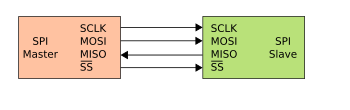
The SPI bus specifies four logic signals:
- SCLK: Serial Clock (output from master);
- MOSI; SIMO: Master Output, Slave Input (output from master);
- MISO; SOMI: Master Input, Slave Output (output from slave);
- SS: Slave Select (active low, output from master).
Alternative naming conventions are also widely used:
- SCK; CLK: Serial Clock (output from master)
- SDI; DI, DIN, SI: Serial Data In; Data In, Serial In
- SDO; DO, DOUT, SO: Serial Data Out; Data Out, Serial Out
- nCS, CS, CSB, CSN, nSS, STE: Chip Select, Slave Transmit Enable (active low, output from master)
The SDI/SDO (DI/DO, SI/SO) convention requires that SDO on the master be connected to SDI on the slave, and vice-versa. Chip select polarity is rarely active high, although some notations (such as SS or CS instead of nSS or nCS) suggest otherwise.
- SPI port pin names for particular IC products may differ from those depicted in these illustrations.
[edit]Operation
The SPI bus can operate with a single master device and with one or more slave devices.
If a single slave device is used, the SS pin may be fixed to logic low if the slave permits it. Some slaves require the falling edge (high→low transition) of the chip select to initiate an action such as the Maxim MAX1242 ADC, which starts conversion on said transition. With multiple slave devices, an independent SS signal is required from the master for each slave device.
Most slave devices have tri-state outputs so their MISO signal becomes high impedance ("disconnected") when the device is not selected. Devices without tri-state outputs can't share SPI bus segments with other devices; only one such slave could talk to the master, and only its chip select could be activated.
[edit]Data transmission
To begin a communication, the master first configures the clock, using a frequency less than or equal to the maximum frequency the slave device supports. Such frequencies are commonly in the range of 1–70 MHz.
The master then pulls the chip select low for the desired chip. If a waiting period is required (such as for analog-to-digital conversion) then the master must wait for at least that period of time before starting to issue clock cycles.
During each SPI clock cycle, a full duplex data transmission occurs:
- the master sends a bit on the MOSI line; the slave reads it from that same line
- the slave sends a bit on the MISO line; the master reads it from that same line
Not all transmissions require all four of these operations to be meaningful but they do happen.
Transmissions normally involve two shift registers of some given word size, such as eight bits, one in the master and one in the slave; they are connected in a ring. Data are usually shifted out with the most significant bit first, while shifting a new least significant bit into the same register. After that register has been shifted out, the master and slave have exchanged register values. Then each device takes that value and does something with it, such as writing it to memory. If there is more data to exchange, the shift registers are loaded with new data and the process repeats.
Transmissions may involve any number of clock cycles. When there are no more data to be transmitted, the master stops toggling its clock. Normally, it then deselects the slave.
Transmissions often consist of 8-bit words, and a master can initiate multiple such transmissions if it wishes/needs. However, other word sizes are also common, such as 16-bit words for touchscreen controllers or audio codecs, like the TSC2101 from Texas Instruments; or 12-bit words for many digital-to-analog or analog-to-digital converters.
Every slave on the bus that hasn't been activated using its chip select line must disregard the input clock and MOSI signals, and must not drive MISO. The master must select only one slave at a time.
[edit]Clock polarity and phase

In addition to setting the clock frequency, the master must also configure the clock polarity and phase with respect to the data. Freescale's SPI Block Guide[1] names these two options as CPOL and CPHA respectively, and most vendors have adopted that convention.
The timing diagram is shown to the right. The timing is further described below and applies to both the master and the slave device.
- At CPOL=0 the base value of the clock is zero
- For CPHA=0, data are captured on the clock's rising edge (low→high transition) and data are propagated on afalling edge (high→low clock transition).
- For CPHA=1, data are captured on the clock's falling edge and data are propagated on a rising edge.
- At CPOL=1 the base value of the clock is one (inversion of CPOL=0)
- For CPHA=0, data are captured on clock's falling edge and data are propagated on a rising edge.
- For CPHA=1, data are captured on clock's rising edge and data are propagated on a falling edge.
That is, CPHA=0 means sample on the leading (first) clock edge, while CPHA=1 means sample on the trailing (second) clock edge, regardless of whether that clock edge is rising or falling. Note that with CPHA=0, the data must be stable for a half cycle before the first clock cycle. For all CPOL and CPHA modes, the initial clock value must be stable before the chip select line goes active.
Also, note that "data is read" in this document more typically means "data may be read". The MOSI and MISO signals are usually stable (at their reception points) for the half cycle until the next clock transition. SPI master and slave devices may well sample data at different points in that half cycle.
This adds more flexibility to the communication channel between the master and slave.
Some products use different naming conventions. For example, the TI MSP430 uses the name UCCKPL instead of CPOL, and its UCCKPH is the inverse of CPHA. When connecting two chips together, carefully examine the clock phase initialization values to be sure of using the right settings.
[edit]Mode numbers
The combinations of polarity and phases are often referred to as modes which are commonly numbered according to the following convention, with CPOL as the high order bit and CPHA as the low order bit:
Another commonly used notation represents the mode as a (CPOL,CPHA) tuple, e.g. the value '(0,1)' would indicate CPOL=0 and CPHA=1
[edit]Independent slave SPI configuration
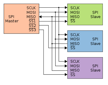
In the independent slave configuration, there is an independent chip select line for each slave. This is the way SPI is normally used. Since the MISO pins of the slaves are connected together, they are required to be tri-state pins.
[edit]Daisy chain SPI configuration
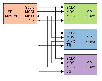
Some products with SPI bus are designed to be capable of being connected in a daisy chain configuration, the first slave output being connected to the second slave input, etc. The SPI port of each slave is designed to send out during the second group of clock pulses an exact copy of what it received during the first group of clock pulses. The whole chain acts as an SPI communication shift register; daisy chaining is often done with shift registers to provide a bank of inputs or outputs through SPI . Such a feature only requires a single SS line from the master, rather than a separate SS line for each slave .[2]
Applications (discussed later) that require a daisy chain configuration include SGPIO and JTAG.
[edit]Valid SPI communications
Some slave devices are designed to ignore any SPI communications in which the number of clock pulses is greater than specified. Others don't care, ignoring extra inputs and continuing to shift the same output bit. It is common for different devices to use SPI communications with different lengths, as, for example, when SPI is used to access the scan chain of a digital IC by issuing a command word of one size (perhaps 32 bits) and then getting a response of a different size (perhaps 153 bits, one for each pin in that scan chain).
[edit]Interrupts
SPI devices sometimes use another signal line to send an interrupt signal to a host CPU. Examples include pen-down interrupts from touchscreen sensors, thermal limit alerts from temperature sensors, alarms issued by real time clock chips, SDIO, and headset jack insertions from the sound codec in a cell phone. Interrupts are not covered by the SPI standard; their usage is neither forbidden nor specified by the standard.
[edit]Example of bit-banging the SPI master protocol
Below is an example of bit-banging the SPI protocol as an SPI master with CPOL=0, CPHA=0, and eight bits per transfer. The example is written in the C programming language. Because this is CPOL=0 the clock must be pulled low before the chip select is activated. The chip select line must be activated, which normally means being toggled low, for the peripheral before the start of the transfer, and then deactivated afterwards. Most peripherals allow or require several transfers while the select line is low; this routine might be called several times before deselecting the chip.
unsigned char SPIBitBang8BitsMode0(unsigned char byte){ unsigned char bit; for (bit = 0; bit < 8; bit++) { /* write MOSI on trailing edge of previous clock */ if (byte & 0x80) SETMOSI(); else CLRMOSI(); byte <<= 1; /* half a clock cycle before leading/rising edge */ SPIDELAY(SPISPEED/2); SETCLK(); /* half a clock cycle before trailing/falling edge */ SPIDELAY(SPISPEED/2); /* read MISO on trailing edge */ byte |= READMISO(); CLRCLK(); } return byte;}
[edit]Pros and cons of SPI
[edit]Advantages
- Full duplex communication
- Higher throughput than I²C or SMBus
- Complete protocol flexibility for the bits transferred
- Not limited to 8-bit words
- Arbitrary choice of message size, content, and purpose
- Extremely simple hardware interfacing
- Typically lower power requirements than I²C or SMBus due to less circuitry (including pullups)
- No arbitration or associated failure modes
- Slaves use the master's clock, and don't need precision oscillators
- Slaves don't need a unique address -- unlike I²C or GPIB or SCSI
- Transceivers are not needed
- Uses only four pins on IC packages, and wires in board layouts or connectors, much less than parallel interfaces
- At most one "unique" bus signal per device (chip select); all others are shared
- Signals are unidirectional allowing for easy Galvanic isolation
[edit]Disadvantages
- Requires more pins on IC packages than I²C, even in the "3-Wire" variant
- No in-band addressing; out-of-band chip select signals are required on shared buses
- No hardware flow control by the slave (but the master can delay the next clock edge to slow the transfer rate)
- No hardware slave acknowledgment (the master could be "talking" to nothing and not know it)
- Supports only one master device
- No error-checking protocol is defined
- Generally prone to noise spikes causing faulty communication
- Without a formal standard, validating conformance is not possible
- Only handles short distances compared to RS-232, RS-485, or CAN-bus
[edit]Applications
The board real estate savings compared to a parallel I/O bus are significant, and have earned SPI a solid role in embedded systems. That is true for most system-on-a-chipprocessors, both with higher end 32-bit processors such as those using ARM, MIPS, or PowerPC and with other microcontrollers such as the AVR, PIC, and MSP430. These chips usually include SPI controllers capable of running in either master or slave mode. In-system programmable AVR controllers (including blank ones) can be programmed using an SPI interface.[3]
Chip or FPGA based designs sometimes use SPI to communicate between internal components; on-chip real estate can be as costly as its on-board cousin.
The full-duplex capability makes SPI very simple and efficient for single master/single slave applications. Some devices use the full-duplex mode to implement an efficient, swift data stream for applications such as digital audio, digital signal processing, or telecommunications channels, but most off-the-shelf chips stick to half-duplex request/response protocols.
SPI is used to talk to a variety of peripherals, such as
- Sensors: temperature, pressure, ADC, touchscreens, video game controllers
- Control devices: audio codecs, digital potentiometers, DAC
- Camera lenses: Canon EF lens mount
- Communications: Ethernet, USB, USART, CAN, IEEE 802.15.4, IEEE 802.11, handheld video games
- Memory: flash and EEPROM
- Real-time clocks
- LCD displays, sometimes even for managing image data
- Any MMC or SD card (including SDIO variant)
For high performance systems, FPGAs sometimes use SPI to interface as a slave to a host, as a master to sensors, or for flash memory used to bootstrap if they are SRAM-based.
JTAG is essentially an application stack for a 3-wire SPI flavor, using different signal names[citation needed]: TCK not SCK, TDI not MOSI, TDO not MISO. It defines a state machine (driven by a TMS signal instead of a chip select line), protocol messages, a core command set, the ability to daisy-chain devices in a "scan chain", and how vendors define new commands. The devices in a scan chain are initially treated as a single device, and transitions on TMS update their state machines; once the individual devices are identified, commands may be issued that affect only one device in that scan chain. Different vendors use different JTAG connectors. Bit strings used in JTAG are often long and not multiples of 8 bit words; for example, a boundary scan reports signal state on each of several hundred pins.
SGPIO is essentially another (incompatible) application stack for SPI designed for particular backplane management activities[citation needed]. SGPIO uses 3-bit messages.
[edit]Standards
The SPI bus is a de facto standard. However, the lack of a formal standard is reflected in a wide variety of protocol options. Different word sizes are common. Every device defines its own protocol, including whether or not it supports commands at all. Some devices are transmit-only; others are receive-only. Chip selects are sometimes active-high rather than active-low. Some protocols send the least significant bit first.
Some devices even have minor variances from the CPOL/CPHA modes described above. Sending data from slave to master may use the opposite clock edge as master to slave. Devices often require extra clock idle time before the first clock or after the last one, or between a command and its response. Some devices have two clocks, one to "capture" or "display" data, and another to clock it into the device. Many of these "capture clocks" run from the chip select line.
Some devices require an additional flow control signal from slave to master, indicating when data are ready. This leads to a "five wire" protocol instead of the usual four. Such a "ready" or "enable" signal is often active-low, and needs to be enabled at key points such as after commands or between words. Without such a signal, data transfer rates may need to be slowed down significantly, or protocols may need to have "dummy bytes" inserted, to accommodate the worst case for the slave response time. Examples include initiating an ADC conversion, addressing the right page of flash memory, and processing enough of a command that device firmware can load the first word of the response. (Many SPI masters don't support that signal directly, and instead rely on fixed delays.)
Many SPI chips only support messages that are multiples of 8 bits. Such chips can not interoperate with the JTAG or SGPIO protocols, or any other protocol that requires messages that are not multiples of 8 bits.
There are even hardware-level differences. Some chips combine MOSI and MISO into a single data line (SI/SO); this is sometimes called "3-Wire" signaling (in contrast to normal "4-wire" SPI). Another SPI flavor removes the chip select line, managing protocol state machine entry/exit using other methods; this isn't usually called 3-Wire though. Anyone needing an external connector for SPI defines their own -- UEXT, JTAG connector, Secure Digital card socket, etc. . Signal levels depend entirely on the chips involved.
[edit]Development tools
When developing or troubleshooting systems using SPI, visibility at the level of hardware signals can be important.
[edit]Host adapters
There are a number of USB hardware solutions to provide computers, running Linux, Mac, or Windows, SPI master and/or slave capabilities. A SPI Host Adapter lets the user play the role of a master on a SPI bus directly from PC. They are used for embedded system, chip (FPGA/ASIC/SoC) and peripheral testing, programming and debug. Because SPI coexists with other buses such as I²C, SPI Host Adapters often have more capabilities (I²C, GPIO, custom protocol support) in addition to pure SPI protocol support.
[edit]Protocol analyzers
SPI Protocol Analyzers are tools which sample a SPI bus and decode the electrical signals to provide a higher-level view of the data being transmitted on a specific bus.
[edit]Oscilloscopes
Every major scope vendor offers scope-based triggering and protocol decode for SPI. Most support 2-, 3-, and 4-wire SPI. The trigger and decode capability is typically offered as a for-pay scope application. SPI signals can be accessed via analog scope channels or with digital MSO channels.
[edit]Logic analyzers
When developing and/or troubleshooting the SPI bus, examination of hardware signals can be very important. Logic analyzers are tools which collect, analyze, decode, store signals so people can view the high-speed waveforms at their leisure. Logic analyzers display time-stamps of each signal level change, which can help find protocol problems. Most logic analyzers have the capability to decode bus signals into high-level protocol data and show ASCII data.
[edit]Related terms
[edit]Queued serial peripheral interface (QSPI)
The queued serial peripheral interface (QSPI) is one type of SPI controller, not another bus type. It uses a data queue with programmable queue pointers allowing some data transfers without CPU intervention.[4] It also has a wrap-around mode allowing continuous transfers to and from the queue with no CPU intervention. As a result, the peripherals appear to the CPU as memory-mapped parallel devices. This feature is useful in applications such as control of an A/D converter. Other programmable features in QSPI are chip selects and transfer length/delay.
SPI controllers from different vendors support different feature sets; such DMA queues are not uncommon, although they may be associated with separate DMA engines rather than the SPI controller itself.[5] Most SPI master controllers integrate support for up to four chip selects,[6] although some require chip selects to be managed separately through GPIO lines.
[edit]Microwire
Microwire is essentially a predecessor of SPI. It's a strict subset: half duplex, and using SPI mode 0. (Microwire-Plus supports other SPI modes.) Microwire chips tend to need slower clock rates than newer SPI versions; perhaps 2 MHz vs. 20 MHz. Some Microwire chips also support a 3-Wire mode (see below), which fits neatly with the restriction to half duplex.
[edit]3-wire serial buses
As mentioned above, one variant of SPI uses single bidirectional data line (Slave Out/Slave IN, called SISO) instead of two unidirectional ones (MOSI and MISO). Clearly, this variant is restricted to a half duplex mode. It tends to be used for lower performance parts, such as small EEPROMs used only during system startup and certain sensors, and Microwire. As of this writing, few SPI master controllers support this mode; although it can often be easily bit-banged in software.
When someone says a part supports SPI or Microwire, you can normally assume that means the four-wire version.
However, when someone talks about a part supporting a 3-wire serial bus you should always find out what it means: standard 4-wire SPI, without the chip select pin from that count, since most buses use chip selects but only three wires carry "real" signals; (More, sometimes with an unshared SPI bus segment the device's chip select will be hard-wired as "always selected".) "real" 3-wire SPI; or even a RS232 cable with RXD, TXD, and shield/ground, or an application-specific signaling scheme.
[edit]Multi I/O SPI
As opposed to 3-wire serial buses, multi I/O SPI uses multiple parallel data lines (e.g. IO0 to IO3) to increase throughput. Dual I/O SPI using two data lines has comparable throughput to fast single I/O (MISO/MOSI). Quad I/O SPI using four data lines has approximately double the throughput.[7] Multi I/O SPI devices tend to be half duplex similar to 3-Wire devices to avoid adding too many pins. These serial memory devices combine the advantage of more speed with reduced pin count as compared to parallel memory.
[edit]See also
- I2C, sometimes called "2-wire" bus
- 1-Wire
- Microwire
- UNI/O
- Computer bus
- Controller Area Network
- Serial communications
- Synchronous Serial Port (SSP)
- Peripheral
- Interface
[edit]References
- ^ SPI Block Guide V03.06, Freescale Semiconductor
- ^ Maxim-IC application note 3947: "Daisy-Chaining SPI Devices"
- ^ AVR910 - In-system programming
- ^ Queued Serial Module Reference Manual, Freescale Semiconductor
- ^ Such as with the MultiChannel Serial Port Interface, or McSPI, used in Texas Instruments OMAP chips. Download just the chapter about the SPI controller, if you want a good example of a highly engineered modern controller.
- ^ Such at the SPI controller on Atmel AT91 chips like the at91sam9G20, which is much simpler than TI's McSPI.
- ^ Serial Peripheral Interface (SPI) Flash Memory Backgrounder, Spansion
[edit]External links
- Introduction to Serial Peripheral Interface
- Introduction to SPI and I2C protocols
- Serial buses information page
- SPI Introduction with helpful diagrams
- Serial Flash Lots of good information on SPI part manufacturers and models.
- SPI - PICmicro Serial Peripheral Interface, Microchip (company) tutorial on SPI.
- OpenCores Open Source implementation of SPI written in Verilog; simpler MC68HC11 version
- SPI flash memory controller, HDL Design House
- SPI Host Adapter - Background Information
- System bus
- Front-side bus
- Back-side bus
- Daisy chain
- Control bus
- Address bus
- Bus contention
- Plug and play
- List of bus bandwidths
- S-100 bus
- Unibus
- VAXBI
- MBus
- STD Bus
- SMBus
- Q-Bus
- ISA
- Zorro II
- Zorro III
- CAMAC
- FASTBUS
- LPC
- HP Precision Bus
- EISA
- VME
- VXI
- NuBus
- TURBOchannel
- MCA
- SBus
- VLB
- PCI
- PXI
- HP GSC bus
- CoreConnect
- InfiniBand
- UPA
- PCI-X
- AGP
- PCI Express
- Intel QuickPath Interconnect
- HyperTransport
- PC Card
- ExpressCard
- Multidrop bus
- AMBA
- Wishbone
- ST-506
- ESDI
- SMD
- Parallel ATA (PATA)
- DMA
- SSA
- HIPPI
- USB MSC
- FireWire (1394)
- Serial ATA (SATA)
- eSATA
- SCSI
- Parallel SCSI
- Serial Attached SCSI (SAS)
- Fibre Channel (FC)
- iSCSI
- Apple Desktop Bus
- HIL
- MIDI
- Multibus
- RS-232 (serial port)
- DMX512-A
- IEEE-488 (GPIB)
- EIA/RS-422
- IEEE-1284 (parallel port)
- UNI/O
- ACCESS.bus
- 1-Wire
- I²C
- SPI
- EIA/RS-485
- Parallel SCSI
- Profibus
- USB
- FireWire (1394)
- Fibre Channel
- Camera Link
- External PCI Express x16
- Thunderbolt
Note: interfaces are listed in speed ascending order (roughly), the interface at the end of each section should be the fastest
- Serial Peripheral Interface Bus · Motorola SPI ARM PL022 控制器驱动移植 SPI接口的SD卡调试
- SPI(Serial Peripheral interface)
- spi(serial peripheral interface)
- SPI - Serial Peripheral Interface
- SPI (Serial Peripheral Interface)
- Serial Peripheral Interface (SPI)
- SPI(Serial Peripheral Interface)串行外设接口
- STM32----------SPI(Serial Peripheral Interface)
- 杂记:Atmel sama5d3 Serial Peripheral Interface (SPI)
- SPI—— Serial Peripheral interface
- Serial Peripheral Interface Bus
- Serial Peripheral Interface驱动
- spi模式sd卡的linux设备驱动移植
- SPI方式驱动SD卡的方法
- 基于SPI模式的SD卡驱动
- SD卡的SPI模式的调试
- stm32 SD卡 SPI驱动以及fatfs移植
- 单片机spi驱动SD卡
- 在排序数组中寻找两个数使其和等于给定数
- HtmlEditor问题总结
- MyEclipse6.5安装SVN插件的三种方法
- TextView一直显示跑马灯效果
- Nginx配置中运行与启动的详细介绍
- Serial Peripheral Interface Bus · Motorola SPI ARM PL022 控制器驱动移植 SPI接口的SD卡调试
- 教你修改Oracle数据库的连接数
- sql server2005 导入.mdf 错误5120
- [jQuery]使用jQuery.Validate进行客户端验证——不使用微软验证控件的理由-目录及简介
- 仅通过崩溃地址找出源代码的出错行
- (转载)Building a Website with PHP, MySQL and jQuery Mobile, Part 1
- 用adb上传so文件到/system/lib下
- 阅读《The C++ Programming Language (Special Edition) 十周年中文纪念版》
- 实习日记026(8月22日)