How Computers Boot Up
来源:互联网 发布:李炎恢php第三季 编辑:程序博客网 时间:2024/05/18 06:18
The previous post described motherboards and the memory map in Intel computers to set the scene for the initial phases of boot. Booting is an involved, hacky, multi-stage affair – fun stuff. Here’s an outline of the process:
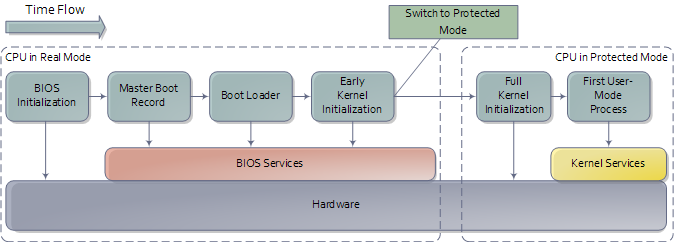
An outline of the boot sequence
Things start rolling when you press the power button on the computer (no! do tell!). Once the motherboard is powered up it initializes its own firmware – the chipset and other tidbits – and tries to get the CPU running. If things fail at this point (e.g., the CPU is busted or missing) then you will likely have a system that looks completely dead except for rotating fans. A few motherboards manage to emit beeps for an absent or faulty CPU, but the zombie-with-fans state is the most common scenario based on my experience. Sometimes USB or other devices can cause this to happen: unplugging allnon-essential devices is a possible cure for a system that was working and suddenly appears dead like this. You can then single out the culprit device by elimination.
If all is well the CPU starts running. In a multi-processor or multi-core system one CPU is dynamically chosen to be the bootstrap processor (BSP) that runs all of the BIOS and kernel initialization code. The remaining processors, called application processors (AP) at this point, remain halted until later on when they are explicitly activated by the kernel. Intel CPUs have been evolving over the years but they’re fully backwards compatible, so modern CPUs can behave like the original 1978 Intel 8086, which is exactly what they do after power up. In this primitive power up state the processor is in real mode with memory paging disabled. This is like ancient MS-DOS where only 1 MB of memory can be addressed and any code can write to any place in memory – there’s no notion of protection or privilege.
Most registers in the CPU have well-defined values after power up, including the instruction pointer (EIP) which holds the memory address for the instruction being executed by the CPU. Intel CPUs use a hack whereby even though only 1MB of memory can be addressed at power up, a hidden base address (an offset, essentially) is applied to EIP so that the first instruction executed is at address 0xFFFFFFF0 (16 bytes short of the end of 4 gigs of memory and well above one megabyte). This magical address is called the reset vector and is standard for modern Intel CPUs.
The motherboard ensures that the instruction at the reset vector is a jump to the memory location mapped to the BIOS entry point. This jump implicitly clears the hidden base address present at power up. All of these memory locations have the right contents needed by the CPU thanks to the memory map kept by the chipset. They are all mapped to flash memory containing the BIOS since at this point the RAM modules have random crap in them. An example of the relevant memory regions is shown below:
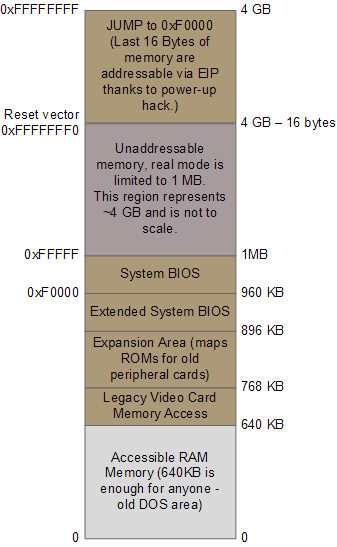
Important memory regions during boot
The CPU then starts executing BIOS code, which initializes some of the hardware in the machine. Afterwards the BIOS kicks off the Power-on Self Test (POST) which tests various components in the computer. Lack of a working video card fails the POST and causes the BIOS to halt and emit beeps to let you know what’s wrong, since messages on the screen aren’t an option. A working video card takes us to a stage where the computer looks alive: manufacturer logos are printed, memory starts to be tested, angels blare their horns. Other POST failures, like a missing keyboard, lead to halts with an error message on the screen. The POST involves a mixture of testing and initialization, including sorting out all the resources – interrupts, memory ranges, I/O ports – for PCI devices. Modern BIOSes that follow the Advanced Configuration and Power Interface build a number of data tables that describe the devices in the computer; these tables are later used by the kernel.
After the POST the BIOS wants to boot up an operating system, which must be found somewhere: hard drives, CD-ROM drives, floppy disks, etc. The actual order in which the BIOS seeks a boot device is user configurable. If there is no suitable boot device the BIOS halts with a complaint like “Non-System Disk or Disk Error.” A dead hard drive might present with this symptom. Hopefully this doesn’t happen and the BIOS finds a working disk allowing the boot to proceed.
The BIOS now reads the first 512-byte sector (sector zero) of the hard disk. This is called the Master Boot Record and it normally contains two vital components: a tiny OS-specific bootstrapping program at the start of the MBR followed by a partition table for the disk. The BIOS however does not care about any of this: it simply loads the contents of the MBR into memory location 0x7c00 and jumps to that location to start executing whatever code is in the MBR.
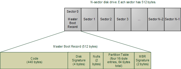
Master Boot Record
The specific code in the MBR could be a Windows MBR loader, code from Linux loaders such as LILO or GRUB, or even a virus. In contrast the partition table is standardized: it is a 64-byte area with four 16-byte entries describing how the disk has been divided up (so you can run multiple operating systems or have separate volumes in the same disk). Traditionally Microsoft MBR code takes a look at the partition table, finds the (only) partition marked as active, loads the boot sector for thatpartition, and runs that code. The boot sector is the first sector of a partition, as opposed to the first sector for the whole disk. If something is wrong with the partition table you would get messages like “Invalid Partition Table” or “Missing Operating System.” This message does not come from the BIOS but rather from the MBR code loaded from disk. Thus the specific message depends on the MBR flavor.
Boot loading has gotten more sophisticated and flexible over time. The Linux boot loaders Lilo and GRUB can handle a wide variety of operating systems, file systems, and boot configurations. Their MBR code does not necessarily follow the “boot the active partition” approach described above. But functionally the process goes like this:
- The MBR itself contains the first stage of the boot loader. GRUB calls this stage 1.
- Due to its tiny size, the code in the MBR does just enough to load another sector from disk that contains additional boostrap code. This sector might be the boot sector for a partition, but could also be a sector that was hard-coded into the MBR code when the MBR was installed.
- The MBR code plus code loaded in step 2 then read a file containing the second stage of the boot loader. In GRUB this is GRUB Stage 2, and in Windows Server this is c:\NTLDR. If step 2 fails in Windows you’d get a message like “NTLDR is missing”. The stage 2 code then reads a boot configuration file (e.g., grub.conf in GRUB, boot.ini in Windows). It then presents boot choices to the user or simply goes ahead in a single-boot system.
- At this point the boot loader code needs to fire up a kernel. It must know enough about file systems to read the kernel from the boot partition. In Linux this means reading a file like “vmlinuz-2.6.22-14-server” containing the kernel, loading the file into memory and jumping to the kernel bootstrap code. In Windows Server 2003 some of the kernel start-up code is separate from the kernel image itself and is actually embedded into NTLDR. After performing several initializations, NTDLR loads the kernel image from file c:\Windows\System32\ntoskrnl.exe and, just as GRUB does, jumps to the kernel entry point.
There’s a complication worth mentioning (aka, I told you this thing is hacky). The image for a current Linux kernel, even compressed, does not fit into the 640K of RAM available in real mode. My vanilla Ubuntu kernel is 1.7 MB compressed. Yet the boot loader must run in real mode in order to call the BIOS routines for reading from the disk, since the kernel is clearly not available at that point. The solution is the venerable unreal mode. This is not a true processor mode (I wish the engineers at Intel were allowed to have fun like that), but rather a technique where a program switches back and forth between real mode and protected mode in order to access memory above 1MB while still using the BIOS. If you read GRUB source code, you’ll see these transitions all over the place (look under stage2/ for calls to real_to_prot and prot_to_real). At the end of this sticky process the loader has stuffed the kernel in memory, by hook or by crook, but it leaves the processor in real mode when it’s done.
We’re now at the jump from “Boot Loader” to “Early Kernel Initialization” as shown in the first diagram. That’s when things heat up as the kernel starts to unfold and set things in motion. The next post will be a guided tour through the Linux Kernel initialization with links to sources at the Linux Cross Reference. I can’t do the same for Windows ![]() but I’ll point out the highlights.
but I’ll point out the highlights.
[Update: cleared up discussion of NTLDR.]
Motherboard Chipsets and the Memory Map
I’m going to write a few posts about computer internals with the goal of explaining how modern kernels work. I hope to make them useful to enthusiasts and programmers who are interested in this stuff but don’t have experience with it. The focus is on Linux, Windows, and Intel processors. Internals are a hobby for me, I have written a fair bit of kernel-mode code but haven’t done so in a while. This first post describes the layout of modern Intel-based motherboards, how the CPU accesses memory and the system memory map.
To start off let’s take a look at how an Intel computer is wired up nowadays. The diagram below shows the main components in a motherboard and dubious color taste:
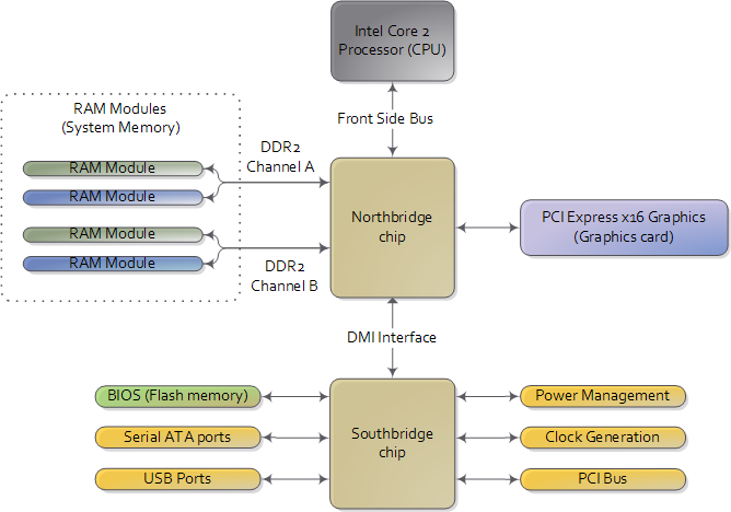
Diagram for modern motherboard. The northbridge and southbridge make up the chipset.
As you look at this, the crucial thing to keep in mind is that the CPU doesn’t really know anything about what it’s connected to. It talks to the outside world through its pins but it doesn’t care what that outside world is. It might be a motherboard in a computer but it could be a toaster, network router, brain implant, or CPU test bench. There are three main ways by which the CPU and the outside communicate: memory address space, I/O address space, and interrupts. We only worry about motherboards and memory for now.
In a motherboard the CPU’s gateway to the world is the front-side bus connecting it to the northbridge. Whenever the CPU needs to read or write memory it does so via this bus. It uses some pins to transmit the physical memory address it wants to write or read, while other pins send the value to be written or receive the value being read. An Intel Core 2 QX6600 has 33 pins to transmit the physical memory address (so there are 233 choices of memory locations) and 64 pins to send or receive data (so data is transmitted in a 64-bit data path, or 8-byte chunks). This allows the CPU to physically address 64 gigabytes of memory (233 locations * 8 bytes) although most chipsets only handle up to 8 gigs of RAM.
Now comes the rub. We’re used to thinking of memory only in terms of RAM, the stuff programs read from and write to all the time. And indeed most of the memory requests from the processor are routed to RAM modules by the northbridge. But not all of them. Physical memory addresses are also used for communication with assorted devices on the motherboard (this communication is calledmemory-mapped I/O). These devices include video cards, most PCI cards (say, a scanner or SCSI card), and also the flash memory that stores the BIOS.
When the northbridge receives a physical memory request it decides where to route it: should it go to RAM? Video card maybe? This routing is decided via the memory address map. For each region of physical memory addresses, the memory map knows the device that owns that region. The bulk of the addresses are mapped to RAM, but when they aren’t the memory map tells the chipset which device should service requests for those addresses. This mapping of memory addresses away from RAM modules causes the classic hole in PC memory between 640KB and 1MB. A bigger hole arises when memory addresses are reserved for video cards and PCI devices. This is why 32-bit OSes haveproblems using 4 gigs of RAM. In Linux the file /proc/iomem neatly lists these address range mappings. The diagram below shows a typical memory map for the first 4 gigs of physical memory addresses in an Intel PC:
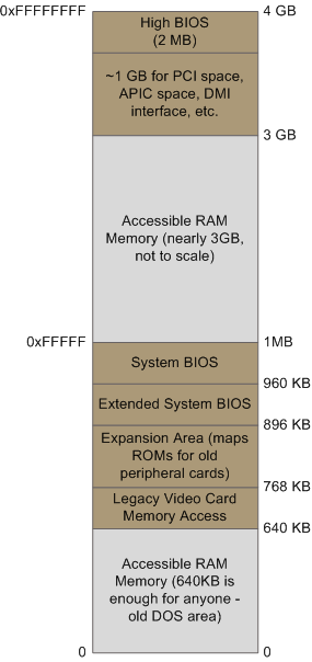
Memory layout for the first 4 gigabytes in an Intel system.
Actual addresses and ranges depend on the specific motherboard and devices present in the computer, but most Core 2 systems are pretty close to the above. All of the brown regions are mapped away from RAM. Remember that these are physical addresses that are used on the motherboard buses. Inside the CPU (for example, in the programs we run and write), the memory addresses are logical and they must be translated by the CPU into a physical address before memory is accessed on the bus.
The rules for translation of logical addresses into physical addresses are complex and they depend on the mode in which the CPU is running (real mode, 32-bit protected mode, and 64-bit protected mode). Regardless of the translation mechanism, the CPU mode determines how much physical memory can be accessed. For example, if the CPU is running in 32-bit mode, then it is only capable of physically addressing 4 GB (well, there is an exception called physical address extension, but ignore it for now). Since the top 1 GB or so of physical addresses are mapped to motherboard devices the CPU can effectively use only ~3 GB of RAM (sometimes less – I have a Vista machine where only 2.4 GB are usable). If the CPU is in real mode, then it can only address 1 megabyte of physical RAM (this is the only mode early Intel processors were capable of). On the other hand, a CPU running in 64-bit mode can physically access 64GB (few chipsets support that much RAM though). In 64-bit mode it is possible to use physical addresses above the total RAM in the system to access the RAM regions that correspond to physical addresses stolen by motherboard devices. This is called reclaiming memory and it’s done with help from the chipset.
That’s all the memory we need for the next post, which describes the boot process from power up until the boot loader is about to jump into the kernel. If you’d like to learn more about this stuff, I highly recommend the Intel manuals. I’m big into primary sources overall, but the Intel manuals in particular are well written and accurate. Here are some:
- Datasheet for Intel G35 Chipset documents a representative chipset for Core 2 processors. This is the main source for this post.
- Datasheet for Intel Core 2 Quad-Core Q6000 Sequence is a processor datasheet. It documents each pin in the processor (there aren’t that many actually, and after you group them there’s really not a lot to it). Fascinating stuff, though some bits are arcane.
- The Intel Software Developer’s Manuals are outstanding. Far from arcane, they explain beautifully all sorts of things about the architecture. Volumes 1 and 3A have the good stuff (don’t be put off by the name, the “volumes” are small and you can read selectively).
- Pádraig Brady suggested that I link to Ulrich Drepper’s excellent paper on memory. It’s great stuff. I was waiting to link to it in a post about memory, but the more the merrier.
- How Computers Boot Up
- How Computers Boot Up
- How Computers Boot Up
- How Computers Boot Up
- How Computers Boot Up
- 计算机如何启动(How Computers Boot Up)
- 计算机是如何启动的 How Computers Boot Up
- How Computers Boot Up -- 计算机是如何启动的
- How Computers Work (8th Edition)
- Configuring Multi-Boot Personal Computers(收藏)
- Computers
- How to deal with “Quota over disk” or “Quota usage warning” during boot up procedure
- How to disable Grub's menu from showing up after failed boot
- how to free up more space in boot partition with Ubuntu16.04
- How Computers Know What We Want — Before We Do
- TED-How we're teaching computers to understand pictures
- how JScript cleans up
- liunx boot up process
- NYOJ - 谁获得了最高奖学金
- 一种将list转换成hashmap的笨办法 其实是将json类型数据转换成键值对
- IT人,请爱惜你的身体
- 设计一个类,我们只能生成该类的一个实例
- 将服务器端的json数组传回客户端(工具类)
- How Computers Boot Up
- myEclipse undeployment failure
- wp8 IsolatedStorageFile XML读写方法
- 什么是存储过程呢?
- jQuery队列控制方法详解queue()/dequeue()/clearQueue()
- PAINTSTRUCT结构
- Introduction to Algorithm(chapter 6)
- Android网络连接判断与处理
- 处理器的乱序和并发执行